


80 WinView/32 Manual Version 2.4.M
User Defined Chip
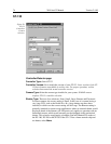
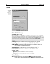
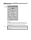
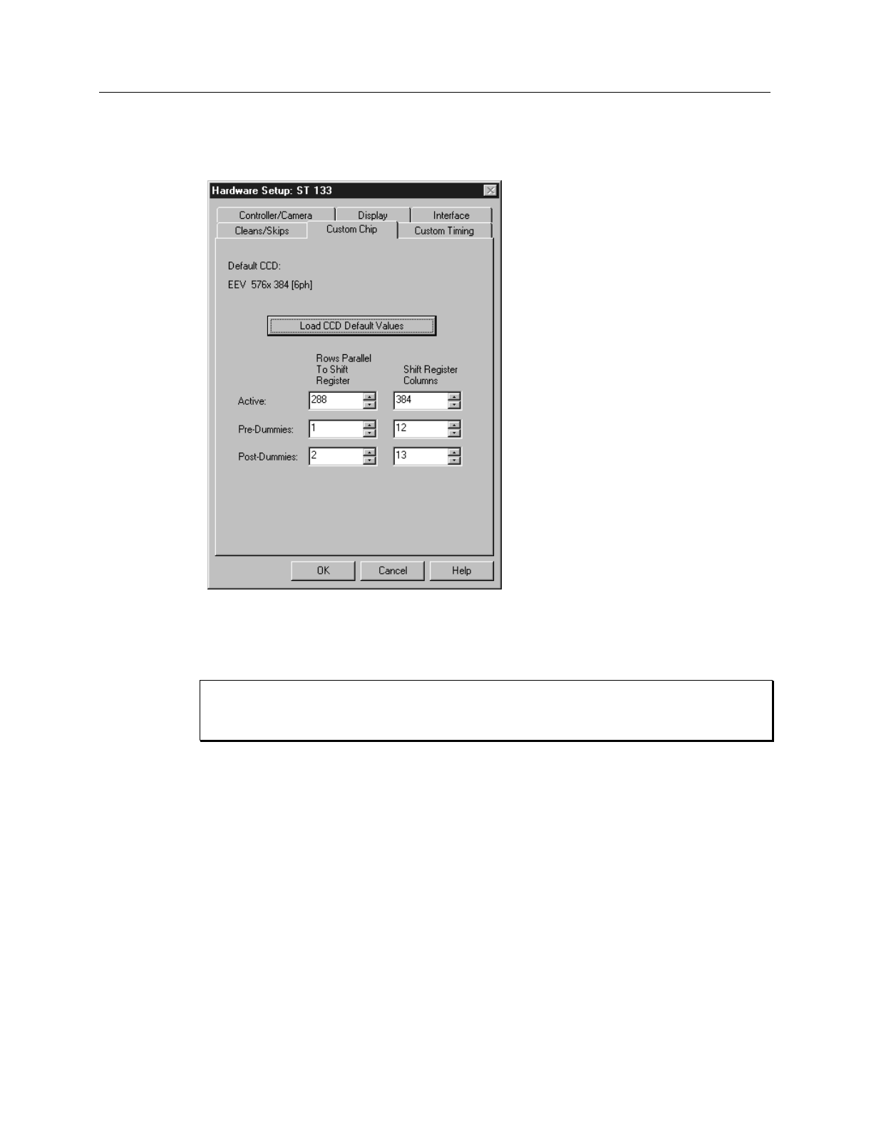
Selecting User Defined Chip on the Controller/Camera tab page makes the Custom Chip
tab page appear (Figure 62). The default values conform to the physical layout of the
CCD array and are optimum for most measurements.
Roper Scientific does not encourage users to change these parameter settings. For most
applications, the default settings will give the best results. We advise contacting the
factory for guidance before customizing the chip definition.
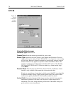
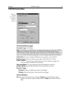
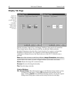
Normally in a CCD array, not all of the pixels are exposed and read out. There is a small
region of “dummy” pixels that bound the active area. These are usually masked.
Although these masked pixels are not normally read out, they could be read out by
changing the chip definition in software. For example, in the case of the EEV 576 × 384
chip illustrated in Figure 62, the 576 active rows are preceded by one dummy row and
followed by 2 dummy rows. In addition, there are 12 dummy columns on one side of the
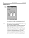
active region and 13 dummy columns on the other side. By changing the chip definition
to increase the active area while decreasing the dummy settings, the dummy cells would
be read out. By doing so, one could measure the dark charge with every readout.
It is also possible to increase image acquisition speed by reducing the size of the active
area in the definition. The result will be faster but lower resolution data acquisition.
Operating in this mode would ordinarily require that the chip be masked so that only the
reduced active area is exposed. This will prevent unwanted charge from spilling into the
active area or being transferred to the output register.
Figure 62.
Custom Chip
tab page.
CAUTION