


8: DMA Controller
GP4020 GPS Baseband Processor Design Manual 91
8 DMA CONTROLLER (DMAC)
The GP4020 contains a DMA controller, which assists the processor to move large blocks of data around a system.
Data transfer between memory blocks, or between memory and a peripheral can be extremely cycle-intensive for a
processor. The ARM processor, for example, requires at least nine clock cycles to move a word of data from one
address in memory to another.
The processor with a source and a destination initialises the DMAC system for the data transfer. On receipt of a
DMA request, the DMA Controller acquires control of the system address and data buses and proceeds to transfer
data until a stop condition is met. The DMA Controller may then be auto-initialised or manually reprogrammed as
desired.
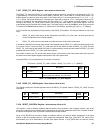
The Base Address for the DMAC is 0xE000 C000. The GP4020 DMAC has two channels. These channels can be
configured to undertake two types of data transfer.
8.1 Single-Addressed (Fly-by) Data transfers
Single-addressed (Fly-by) data transfers are possible between memory and either UARTs 1 or 2.
A Single-addressed Transfer is the faster of the two types of DMA data transfer, in that one data transaction per
bus cycle can be implemented. By its very nature, a single-address may be an area of memory, implying that the
other end of the transfer must be a fixed peripheral, which is signalled using a hardware handshake (dreq and
dack). Refer to Section 6.2.1 in the Firefly MF1 Core Design Manual (DM5003) for details of Single-addressed
transfers.
Each DMAC channel is capable of generating an address and hardware-acknowledge signal for a particular data
transaction. Data is presented to the bus by the source and written to the destination during a single bus
transaction; it is not buffered by the DMA controller. An address is broadcast onto the bus simultaneously.
In the GP4020, hardware handshake signals dack and dreq emanate from each of the two DMAC channels to
control fly-by data transfers with UARTs 1 and 2 as follows:
i) DMAC Channel 1 (dack1 and dreq1) for Data from UART1 RX (received data) to Memory;
ii) DMAC Channel 1 (dack1 and dreq1) for Data from Memory to UART1 TX (transmitted data);
iii) DMAC Channel 2 (dack2 and dreq2) for Data from UART2 RX (received data) to Memory;
iv) DMAC Channel 2 (dack2 and dreq2) for Data from Memory to UART2 TX (transmitted data);
The configuration of the DMAC channels does not allow simultaneous transmit and receive from one UART in fly-by
mode.
8.1.1 Set up example of DMAC for a Fly-by transfer from memory to UART TX
The following example shows the sequence of events required to program and enable the GP4020 DMAC to
provide a Fly-by data transfer from an area of memory to a UART Transmit output.
1) Initialise UART1 (or 2) for data transmission:
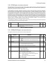
1.1) For the UART 1 (or 2) Serial Control Register (CR):
1.1.1) Set to “1” the Transmit Channel Control bit (bit 1) to enable the UART 1 (or 2) transmit channel.
1.1.2) Clear to ”0” the Clock Source bit (bit 2), to ensure the UART Clock is connected internally to the
UART_CLK source, from the System Clock Generator block (SCG).
1.1.3) Clear to ”0” the Flow Control Type bit (bit 3) of UART Serial Control Register (CR), to enable Software
Flow Control. There are no Hardware Control lines (RTS, CTS) for either UART1 or UART2 bonded
out on the GP4020 device.