


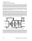
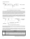
14: System Clock Generator
144 GP4020 GPS Baseband Processor Design Manual
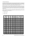
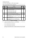
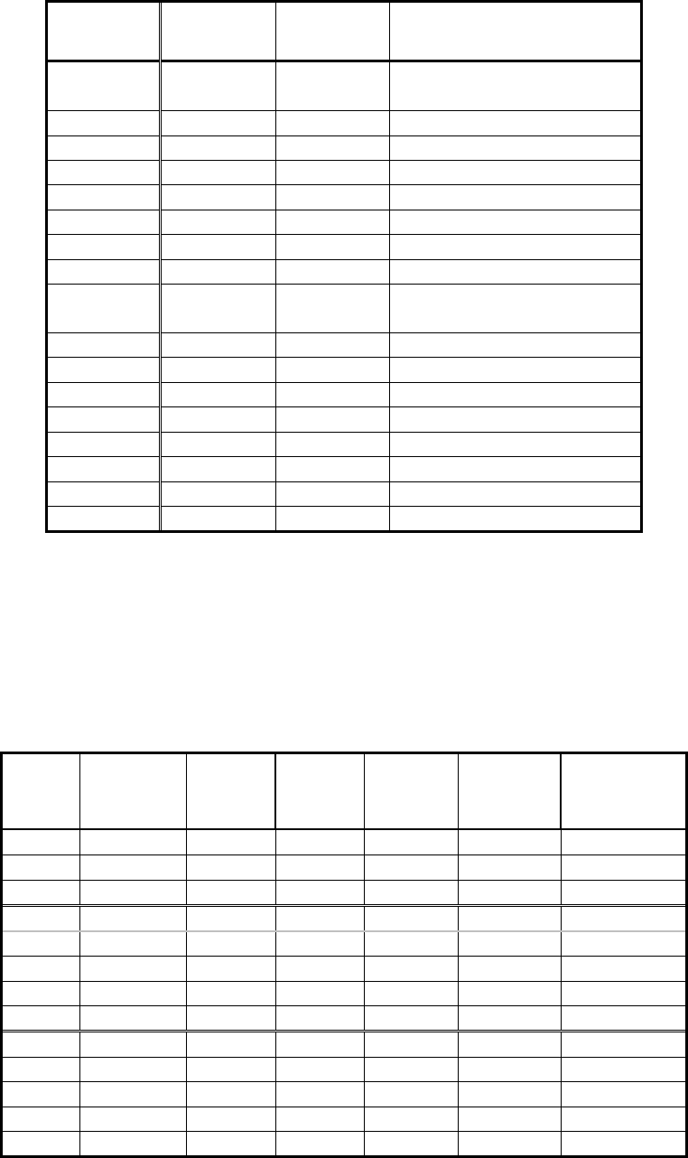
UART_CLK
O/P Freq.
(MHz)
POW_CNTL
register value
PLL_CNTL
register value
Comments
10.0 0x803C 0x197F PLL bypassed and disabled
PLL_CNTL value = reset value
11.25 0x80D8 0x018E
12.5 0x8098 0x09C6
13.75 0x80D8 0x01D2
15.0 0x8058 0x1202
16.25 0x80D8 0x0256
17.5 0x8098 0x0A4A
18.75 0x80D8 0x029A
20.0 0x8036 0x197F PLL bypassed and disabled
PLL_CNTL value = reset value
21.25 0x80D8 0x02DE
22.5 0x8098 0x018E
23.75 0x80D8 0x0362
25.0 0x8058 0x09C6
26.25 0x80D8 0x03A6
27.5 0x8098 0x01D2
28.75 0x80D8 0x03EA
30.0 0x8018 0x1202
Table 14.4 SCG register values for UART_CLK frequencies produced from M_CLK (from RF Front end)
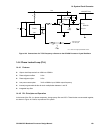
For information of the structure of the POW_CNTL and PLL_CNTL registers, refer to Section 14.6 System Clock
Generator Registers on page 146.
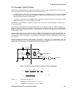
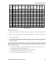
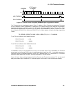
If, the UART_CLK signal is to be derived from an external crystal reference via the on-chip Processor Crystal
Oscillator (frequency inputs between 10.0MHz and 16.0MHz), Table 14.5 below shows the configurations which
can be set-up for the PLL in this case. Note that due to the virtually infinite range of crystal frequencies that can be
used, precise frequencies are NOT shown Table 14.5 below. Remember that any clock multiple can be divided
down to any frequency using the "Divide 1/2/4/8" block which is controlled by the B_CLK_SEL[1:0] register bits.
PLL
Mult
Factor
Desired PLL
output
frequency
Prog.
Divider
Control
DIV[4:0]
PLL
SYNC
MODE
SYNCEN
Charge
Pump
setting
CHP[4:0]
VCO Freq.
Range
VCOD[1:0]
Worst case
settling time.
(µs)
1 10-32MHz 11111 1 00101 11 67
2 10-32MHz 00000 0 01011 11 38
3 10-32MHz 00001 0 10000 11 31
2 20-63MHz 00000 0 00101 10 67
3 20-63MHz 00001 0 01000 10 47
4 20-63MHz 00010 0 01011 10 38
5 20-63MHz 00011 0 01101 10 35
6 20-63MHz 00100 0 10000 10 31
3 40-125MHz 00001 0 00100 01 81
4 40-125MHz 00010 0 00101 01 67
5 40-125MHz 00011 0 00111 01 52
6 40-125MHz 00100 0 01000 01 47
7 40-125MHz 00101 0 01001 01 44