


21: Timing Characteristics
196 GP4020 GPS Baseband Processor Design Manual
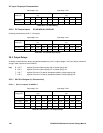
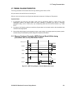
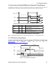
For this example an edge triggered packet transfer (size = 2) is shown.
NOTE: When performing a DMA transfer, memory signals are as per the MPC timing information.
Parameter Min Max Unit Description and notes
Tdreq 0 ns
Dreq setup before B
µILD_CLK
Tdreq_hold 7.5 ns
Dreq hold time after B
µILD_CLK
Tdack 14.2 29.8 ns
B
µILD_CLK to Dack active
Tdackh 11.1 29.0 ns
Dack hold after B
µILD_CLK (Dack1 & Dack2)
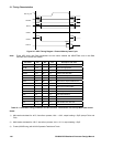
Table 21.3 Simulated DMAC Timing parameters
Notes:
1) MIN results simulated for -40°C, fast silicon process, Vdd = +3.6V, output loading = 50pF, used for input hold.
2) MAX results simulated for +85°C, slow silicon process, Vdd = +3.0 V, output loading = 50pF, used for input
setup.
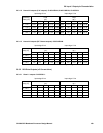
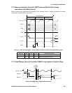
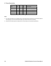
21.4 External interrupt inputs: Timing for Edge sensitivity mode
Interrupts are asynchronous and therefore unaffected by BµILD_CLK.
Interrupts are programmable and timings apply for both rising and falling edges.
Iextint2
Tint_min
Figure 21.5 Interrupt timing
Parameter Min Max Unit Description and notes
Tint_min 5.0 - ns Minimum external interrupt width
Table 21.4 Simulated Interrupt Timing parameters
Note: MIN result simulated for -40°C, fast silicon process, Vdd = +3.6V, output loading = 50pF, used for input
hold.
21.5 External interrupt inputs: Timing for Level sensitivity mode
When Level-sensitive interrupts are programmed, they must remain active until a suitable response is generated.
(i.e. until they have been serviced.) Therefore, please refer to “Firefly MF1 Core Design Manual” for timing
relationship diagrams.