


14: System Clock Generator
GP4020 GPS Baseband Processor Design Manual 141
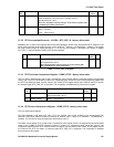
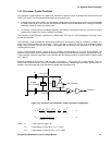
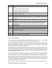
PIN DESCRIPTION
VCOD[1:0] PLL VCO Output Frequency Range selection pin. This input determines which of the 4 frequency ranges are
selected.
'00' operates the VCO between 80MHz and 250MHz;
'01' operates the VCO between 40MHz and 125MHz;
'10' operates the VCO between 20MHz and 63MHz;
'11' operates the VCO between 10MHz and 32MHz
PD
PLL power down and reset pin. When PD is high the PLL is powered down, the ‘CLKOUTB’ output is forced high
and all cells within the PLL are reset.
ENB PLL Enable Bar pin. This pin will power down the PLL if taken high identically to the PD pin.
DIV [4:0] Programmable divider programming bits used for setting up the PLL in clock multiplication mode. These inputs
are binary weighted to give divider settings from 2 to 25. The binary value of ‘n’ will give a divider setting of N =
n+2. For clock synchronisation (divide by 1) set SYNCEN to a ‘1’ and DIV0-4 all to a ‘1’ (to minimise power
consumption).
SYNCEN The PLL is forced into a clock synchronisation mode when pin SYNCEN is tied ‘high’ overriding the programming
bits DIV0-4.
CHP [4:0] Charge pump current setting pins. The internal charge pump current is set by the digital value on these pins
(binary weighted; LSB=CHP0). The charge pump must be correctly programmed to ensure stability of the PLL
control loop. Refer to
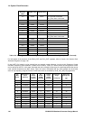
Table 14.2 on page 142, Table 14.3 on page 143 and Table 14.4 on page 144 for
recommended values.
SG1 PLL test control pin.
TM1 PLL test pin 1.
TM2 PLL test pin 2.
PLLAT1 Analog Test Access Pin. During normal operating modes this signal is pulled low by the PLL. It should not be
connected externally to the device.
PLLDT1 Digital Test Access Output pin. The state of this pin must be observable from the device pins during testing of the
PLL.
PLLGND PLL GND pin. This pin connects to the PLL GND supply.
PLLVDD PLL VDD pin. This pin connects to the PLL VDD supply.
Table 14.1 PLL Block Pin Names & Descriptions
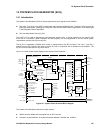
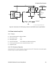
14.4.3 PLL Programming
The PLL charge pump (CHP[4:0]) and feedback divider (DIV[4:0] & SYNCEN) values must be programmed
correctly according to the VCO range selected (VCOD[1:0]) and the clock multiplication ratio.
The maximum output frequency from the PLL can be up to 250MHz. The PLL output frequency will be an integer
multiple of the PLL reference input frequency. The valid frequency input to the PLL from M_CLK can be 10.0MHz,
20MHz or any frequency from 10.0MHz to 16.0MHz as determined by an external crystal connected between
PR_XIN and PR_XOUT on the Processor Crystal Oscillator.
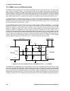
Although the maximum system frequency is going to be much less than the maximum frequency of operation of the
PLL block (250MHz), the wide range of the PLL frequency output gives a wide range of possible UART_CLK output
frequencies, in conjunction with a programmable output stage divider. The smallest step resolution that the SCG
has, is 1.25MHz by virtue of the output divider set to divide by 8, and that the lowest input reference frequency that
the PLL can operate at is 10.0MHz.
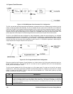
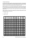
The range of clock frequencies, which can be provided for UART_CLK, using a reference signal derived from
M_CLK, is quite extensive. As an example, the frequencies that can be produced for UART_CLK when the M_CLK
signal derived from the CLK_I and CLK_T signals (40MHz from a RF Front-end) are shown in Table 14.2 below.
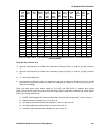
Additional frequencies beyond the specified maximum speed for the GP4020 are also shown in Table 14.3 on page
143. Whilst in normal operation, it is not recommended to exceed the maximum specified operating frequency, the
numbers in this table are shown for experimental purposes. Whilst under certain conditions it may be possible to
run GP4020 above 30MHz, it is not recommended.
Note: Refer to the GP4020 Datasheet (DS5134) for specified limits on the GP4020 maximum operating speed.