


14: System Clock Generator
GP4020 GPS Baseband Processor Design Manual 139
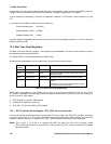
TCXO
10uF
Vcc
To RF Front-end
PLL Ref input
Vcc
GND
10.0MHz
GP4020
PRX_IN
PRX_OUT
Vdd (NOT Vcc)
1M
IC1
100nF 1nF
47nF
100
1V p-p
IC1 = ANY 3.3V High-speed CMOS Inverter.
3.3V p-p
47nF
~0.5V p-p
33
~1k
100nF
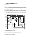
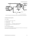
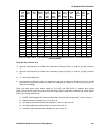
Figure 14.4 Connections of a TCXO frequency reference to the GP4020 Processor Crystal Oscillator
14.4 Phase Locked Loop (PLL)
14.4.1 Features
• Output clock frequencies from 10MHz to 250MHz
• Phase alignment offset: 0.3ns
• Phase alignment jitter: 0.5ns
• Low power consumption: 7mW at 20MHz input, 80MHz output frequency
• Internal programmable divider for clock multiplication between 1 and 25
• Integrated loop filter
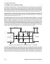
14.4.2 PLL Principles and Operation
At the heart of the PLL is a phase comparator, charge pump, filter and VCO. These blocks are connected together,
as shown in Figure 14.5 below, to produce a PLL system: