


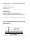
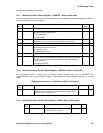


19: System Address Map
GP4020 GPS Baseband Processor Design Manual 183
19.2 GP4020 Firefly MF1 Address Map
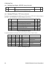
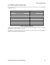
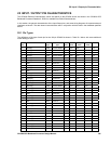
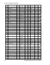
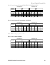
The Firefly MF1 BµILD bus modules have the address map as shown in Table 19.6 below, in the range 0xE000
0000 to 0xE007 FFFF.
ADDRESS RANGE FUNCTION
0xE000 2000 - 0xE000 2FFF System Configuration (including SSM)
0xE000 4000 - 0xE000 4FFF Watchdog (WDOG)
0xE000 5000 - 0xE000 5FFF General purpose I/O block (GPIO)
0xE000 6000 - 0xE000 6FFF Interrupt Controller (INTC)
0xE000 7000 - 0xE000 7FFF Serial Input / Output block (BSIO)
0xE000 8000 - 0xE000 8FFF Memory/Peripheral Controller (MPC)
0xE000 C000 - 0xE000 CFFF DMA Controller (DMAC)
0xE000 E000 - 0xE000 EFFF Timer 1 (TIC1)
0xE000 F000 - 0xE000 FFFF Timer 2 (TIC2)
0xE001 8000 - 0xE001 8FFF UART1
0xE001 9000 - 0xE001 9FFF UART2
All other areas in the range : 0xE000 0000 - 0xFFFF FFFF
Reserved
Table 19.6 Firefly MF1 Address Map
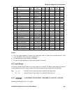
Further details on how to configure all the GP4020 Memory Areas, is described in Section 11 "MEMORY
PERIPHERAL CONTROLLER (MPC)" on page 109.
Further details on Wait-state Generation can be found in Section 3.3.3 of the “Firefly MF1 Core Design Manual”
(DM5003), also available from Zarlink Semiconductor.