


9: GPIO Interface
GP4020 GPS Baseband Processor Design Manual 103
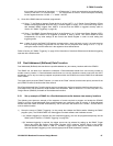
9 GENERAL PURPOSE INPUT OUTPUT (GPIO) INTERFACE
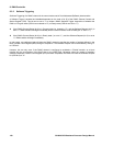
9.1 Introduction
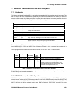
A set of 8 general purpose static input output logic lines are included in the GP4020 to allow multiple static data to
be provided to external features, or allow multiple input data lines to be read. The GPIO pins are multiplexed by the
Peripheral Control Logic (PCL) between the BµILD Serial Input Output (BSIO) lines, and control lines to the
Correlator. Refer to Section 6 "B
µ
ILD SERIAL INPUT OUTPUT (BSIO) INTERFACE" on page 33 and Section 12.4
"Multiplex Logic" on page 119, for further information.
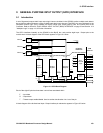
The GPIO interfaces internally on the GP4020 to the BµILD bus, and provides eight Input / Output pins to the
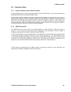
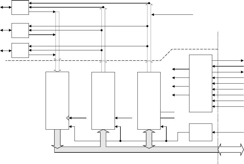
outside world. A block diagram of the GPIO block appears in Figure 9.1 below.
B_DATA [7:0]
Reset
Control
Bus
Decode
Logic
read
only
B_ADDR[3]
B_ADDR[2]
B_WRITE
B_CLK
NCS
B_MODE[2:0]
T = Direction
Data
0 = output
1 = input
oe
op_wr
dir_wr
dir_rdip_rd
rst
rst
write
only
bi-
directional
ARM
BuILD Bus
oe
B_ERROR
B_SIZE[1:0]
B_WAIT
SLEEP_CLKEN
ip_rd
op_wr
dir_wr
dir_rd
TFD
EXTERNAL
INTERFACE
B_DATA[7:0]
Input
Register
rst
8 LINES
Output
Register
8 LINES
Direction
Register
IO PIN 1
IO PIN 2
IO PIN 8
....
8 LINES
F
T
D
F
T
D
F
T
D
GPIO 1
GPIO 2
GPIO 8
Figure 9.1 GPIO Block Diagram
Each of the eight IO pins has three data / control lines associated with it:
F - Input data
D - Output data
T - Tristate output enable/disable. Used to set the data direction into / out of the pin.
A block-diagram of the bi-directional Input / Output interface pin electronics appears in Figure 9.2 below.