


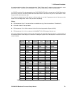

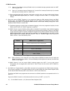

7: 12-Channel Correlator
GP4020 GPS Baseband Processor Design Manual 87
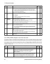
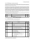
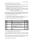
Bit
No.
Mnemonic Description Reset
Value
R/W
3 TM_TEST
Enables Tracking Module Test mode. This permits writes to the registers
which are normally inhibited from write operations, namely
CHx_CARRIER_CYCLE_COUNTER and
CHx_CODE_PHASE_COUNTER registers.
'1' = Enable Tracking Module Test.
'0' = Disable Tracking Module Test.
0W
2 FE_TEST '1' = Enable RF Front End Test mode.
'0' = Disable RF Front End Test mode.
Refer to the text at bottom of this register for more information on RF Front
End Test
.
0W
1 EN_DUMMYTICS Enable DUMMYTICS Input.
'1' = Enable DUMMYTICS input.
'0' = Disable DUMMYTICS input.
(See Note 3)
0W
0 EN_DUMMYDUMP '1' = Enable DUMMYDUMP input.
'0' = Disable DUMMYDUMP input.
(See Note 4)
0W
Table 7.38 CORR TEST_CONTROL Register
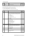
Notes:
1) In EN_SCAN_PATH, the "DISCOP = SCAN_OUT" function may be over–ridden by the DISCOP_
SELECT_100KHZ function of SYSTEM_ SETUP. The MULTI_FN_IO and DISCIO pins will only connect to the
signals identified in this mode if UIM_TEST mode has been set-up using TEST (pin 67(100-pin package)) and
TESTMODE (pin 74 (100-pin package)). Both of these pins should be configured as inputs via the IO_REV
register in the PCL block. Refer to Section 12.7.2 "PCL Input / Output Control register - IO_REV - Memory
Offset 0x00C on page 127, for details.
2) Enables a self-test generator formed from the CH0 Code Generator. The data replaces the SIGN0 and MAG0
inputs. It has a chip rate and phase set by the CH0_CODE_DCO and a carrier frequency set by the
CH0_CARRIER_DCO. The code is set by writing the appropriate start value into the CH0_SATCNTL register,
and the CH0_SLEW_COUNTER can be programmed to delay the start of the code generation by a number of
half code chips. The three most significant bits of the Carrier DCO are decoded to give the SIGN with 50% of
Highs and the MAG with 25% of Highs. The polarity of the data pattern is set by TEST_DATA, EXORed with
the CH0 C/A code.
3) Changes the function of the DISCIP1 input to a DUMMYTIC input. This replaces the TIC from the Timebase
generator so that a TIC effect will only occur when there is a Low to High transition on DISCIP1 (derived from
GPIO[4] (pin 95 (100-pin package))), to latch new Measurement Data. The DISCIP1 input must be held High
for at least 200ns for each DUMMYTIC.
4) Enable DUMMYDUMP signal input. Changes the function of an internal signal (MOTINTELB) to be a
DUMMYDUMP signal (MOTINTELB is derived from DISCIO input (pin 55 (100-pin package)) when UIM_TEST
mode is enabled (refer to PCL documentation)). A DUMMYDUMP will operate in the same way as a normal
DUMP (reset all of the code generators and transfer the contents of all integrators into the Accumulated Data
registers). Each Low to High transition of DISCIO will cause a DUMMYDUMP and if DISCIO is already High
when EN_DUMMYDUMP is set, one will occur immediately. Selecting Dummy dump mode does not inhibit
normal DUMP events. The DISCIO pin must be held High for at least 200ns for each DUMMYDUMP.
7.6.32.1 Details of RF Front End Test mode (FE_TEST)
When FE_TEST is set High this test control forces the SIGN input to channel 11 and the MAG input to channel 5
both to Low. This allows the evaluation of the RF Front end SIGN (on channel 5) and MAG (on channel 11) duty
cycles. The Front end to be tested is selected by the SOURCESEL bits in CH5_SATCNTL and CH11_SATCNTL.