


Index - VI GP4020 GPS Baseband Processor Design Manual
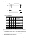
Table of Data Tables
Page
Table 2.1 GP4020 100-pin package dimensions ........................................................................13
Table 2.2 GP4020 100-pin package Signal Descriptions ............................................................16
Table 3.1 Standard 32-bit ARM instruction set ...........................................................................21
Table 3.2 16-bit Thumb instruction set.......................................................................................22
Table 3.3 ARM State General Registers and Program Counter...................................................23
Table 3.4 ARM State Program Status Registers.........................................................................23
Table 3.5 Thumb State General Registers and Program Counter................................................24
Table 3.6 Thumb State Program Status Registers......................................................................24
Table 6.1 BSIO Slave Select Enable Configuration ....................................................................40
Table 6.2 BSIO Register Map....................................................................................................44
Table 6.3 BSIO Configuration Register......................................................................................45
Table 6.4 BSIO Transfer Register..............................................................................................46
Table 6.5 BSIO Mode Register..................................................................................................46
Table 6.6 BSIO Slave Select Register........................................................................................46
Table 6.7 BSIO Status Register.................................................................................................47
Table 6.8 BSIO Interrupt Control Register..................................................................................47
Table 6.9 BSIO Read/Write Buffer Register ...............................................................................48
Table 6.10 BSIO Control Word Buffer Register ..........................................................................48
Table 7.1 12-channel Correlator Carrier DCO outputs ................................................................53
Table 7.2 12-channel correlator (CORR ) Register Map..............................................................65
Table 7.3 CORR Tracking Channel Control Registers Map.........................................................66
Table 7.4 CORR Tracking Channel Data Accumulation Registers Map.......................................67
Table 7.5 CORR Tracking Channel Status Registers Map..........................................................67
Table 7.6 CORR ACCUM_STATUS_A Register.........................................................................68
Table 7.7 CORR ACCUM_STATUS_B Register.........................................................................69
Table 7.8 CORR ACCUM_STATUS_C Register ........................................................................70
Table 7.9 CORR CHx_ACCUM_RESET Register ......................................................................70
Table 7.10 CORR CHx_CARRIER_CYCLE_COUNTER Register...............................................71
Table 7.11 CORR CHx_CARRIER_CYCLE_HIGH Register .......................................................71
Table 7.12 CORR CHx_CARRIER_CYCLE_LOW Register........................................................71
Table 7.13 CORR CHx_CARRIER_DCO_INCR_HIGH Register.................................................72
Table 7.14 CORR CHx_CARRIER_DCO_INCR_LOW Register .................................................72
Table 7.15 CORR CHx_CARRIER_DCO_PHASE Register........................................................73
Table 7.16 CORR CHx_CODE_DCO_INCR_HIGH Register ......................................................73
Table 7.17 CORR CHx_CODE_DCO_INCR_LOW Register.......................................................74