


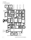
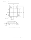
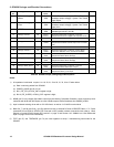
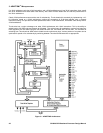
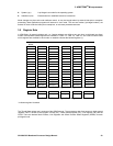

2: GP4020 Package and Electrical Connections
16 GP4020 GPS Baseband Processor Design Manual
Pin
No.
Signal Name Type Circuit
Block
Description Notes
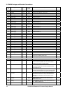
88 TDO / bdiag[2] /
XBurst
I/O JTAG /
SSM
JTAG Test Data Out / SSM Diagnostic
broadcast output bdiag[2] / System Test control
input XBurst
6
89
TMS / bdiag[3] /
XCon
I/O
JTAG /
SSM
JTAG Test Mode Select / SSM Diagnostic
broadcast output bdiag[3] / System Test control
input XCon
6
90 NTRST I
JTAG /
SSM
JTAG Interface Reset or SSM debug interface
multiplex (pins 86, 87, 88, 89).
6
91 GPIO[7] / PLLDT1 I/O GPIO /
SCG PLL
General Purpose Input / Output pin 7.
Can be
multiplexed to SCG PLL Digital Test Output (PLLDT1).
3
92 GPIO[6] I/O GPIO General Purpose Input / Output pin 6. 3
93 GPIO[5] / DISCOP I/O
GPIO /
CORR
General Purpose Input / Output pin 5. Can be
multiplexed to DISCOP discrete output from correlator
core.
3
94 GND PWR
95 GPIO[4] / DISCIP1 I/O
GPIO /
CORR
General Purpose Input / Output pin 4. Also directly
connects to DISCIP1 on the 12-channel correlator.
3
96 GPIO[3] / BSIO_SS[1] I/O GPIO /
BSIO
General Purpose Input / Output pin 3. Can be
multiplexed to BSIO Slave Select[1].
3
97 GPIO[2] / BSIO_SS[0] I/O GPIO /
BSIO
General Purpose Input / Output pin 2. Can be
multiplexed to BSIO Slave Select[0].
3
98 VDD PWR
99 GPIO[1] / BSIO_DATA I/O GPIO /
BSIO
General Purpose Input / Output pin 1. Can be
multiplexed to BSIO Data Input / Output.
3
100 GPIO[0] / BSIO_CLK I/O GPIO /
BSIO
General Purpose Input / Output pin 0. Can be
multiplexed to BSIO_CLK output.
3
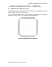
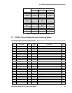
Table 2.2 GP4020 100-pin package Signal Descriptions
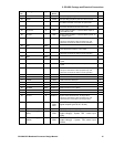
Notes:
1) Hi Impedance is achieved on pins 11 to 18, 20, 21, 23 to 29, 31, 32, 34 to 37 when either:
(a) Data is not being written from GP4020
(b) POWER_GOOD (pin 64) is Low;
(c) Bit 1 ("RF_PD") of POW_CNTL register is high;
(d) Bit 10 ("RF_SLEEP") of POW_CNTL register is High;
2) NSUB (pin 52 is the Upper Byte select output from the Memory Peripheral Controller, when single-chip 16-bit
memories with NUB and NLB inputs are used. NSUB maps to NUB and address line SADD[0] to NLB.
3) Input is tolerant to being driven with a +5V HIGH level, as well as +3.3V HIGH nominal level.
4) Both CLK_T (pin 58) and CLK_I (pin 59) should not have an external DC bias of GREATER than +1.7V. Direct
connection from a GP2010 / GP2015 RF Front-end is NOT possible, without a bias-shift circuit (refer to Block
Diagram of typical GP4020 based GPS receiver" on page 8, and Section 14.2 "40MHz Low Level Differential
Input" on page 136 for more information).
5) TEST (pin 67) and TESTMODE (pin 74) are used together to set-up 3 manufacturing test-modes for the
GP4020: