


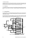
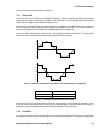

6: BSIO Interface
48 GP4020 GPS Baseband Processor Design Manual
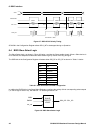
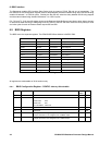
6.9.7 BSIO Read/Write Buffer Register - RWBUF - Memory Offset - 0x0038
Bit
No.
Mnemonic Description Reset
Value
R/W
31:0 RWBUFF 32-bit Read/Write buffer, for word to be sent and received.
Data Transfer can be either byte oriented, or based on a
Word Width configurable between 2- and 32-bits, for the
Read and Write Buffers. When configured as a Word, only
the selected number of lower order bits are employed, with
the remaining higher order bits not used. This is
implemented as a 2 Word by 32-bit FIFO, for both words to
be sent and those received.
All = 0 R/W
Table 6.9 BSIO Read/Write Buffer Register
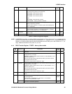
6.9.8
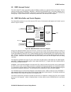
BSIO Control Word Buffer Register - CWBUF - Memory Offset - 0x003C
Bit
No.
Mnemonic Description Reset
Value
R/W
31:0 CONT 32-bit Control Word to be sent. This will be the first word
sent in an operation, if the CWORDSEL bit, in the Mode
Register is set. The width of this word is configurable from
2- to 32-bits via the CWORD bits in the Mode Register.
All = 0 R/W
Table 6.10 BSIO Control Word Buffer Register