


7: 12-Channel Correlator
68 GP4020 GPS Baseband Processor Design Manual
The registers are listed in alphabetical order and not in address order to allow easy reference to each section.
Unless otherwise stated the LSB is bit 0 and the MSB is bit 15 or as far up the register as there is data. Note that
most registers do not have both read and write functions, and many addresses are shared between read–only and
write–only registers having different functions.
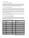
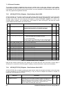
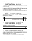
7.6.3 ACCUM_STATUS_A Register - Read Address offset 0x208
ACCUM_STATUS_A is a register containing the state of twelve status bits sampled and latched on the active edge
of every ACCUM_INT. They can also be sampled and latched on request, by performing a write operation to
STATUS. (This is safe only if the interrupts are stopped, by setting INTERRUPT_ENABLE bit to LOW in the
SYSTEM_SETUP register.) The microprocessor must respond to each ACCUM_INT and read the channel
registers before the next DUMP is due in that channel.
Bit
No.
Mnemonic Description Reset
Value
R/W
15 ACCUM_INT Set HIGH at each occurrence of ACCUM_INT; Reset by reading
ACCUM_STATUS_A register. This status bit is reset by a
hardware master reset but not by a software reset (MRB).
0R
14
Not used
'0' when read 0 R
13
Not used
'0' when read 0 R
12
Not used
'0' when read 0 R
11 CH11_NEW_ACCUM_DATA '1' = a DUMP has occurred in Correlator Channel 11, and that
new Accumulated Data is available to be read.
'0' = no new data available.
Each bit is cleared by the trailing edge of a read of the associated
CHx_Q_PROMPT register or by a write to CHx_ACCUM_RESET.
0R
10 CH10_NEW_ACCUM_DATA (as bit 11 but for channel 10) 0 R
9 CH9_NEW_ACCUM_DATA (as bit 11 but for channel 9) 0 R
8 CH8_NEW_ACCUM_DATA (as bit 11 but for channel 8) 0 R
7 CH7_NEW_ACCUM_DATA (as bit 11 but for channel 7) 0 R
6 CH6_NEW_ACCUM_DATA (as bit 11 but for channel 6) 0 R
5 CH5_NEW_ACCUM_DATA (as bit 11 but for channel 5) 0 R
4 CH4_NEW_ACCUM_DATA (as bit 11 but for channel 4) 0 R
3 CH3_NEW_ACCUM_DATA (as bit 11 but for channel 3) 0 R
2 CH2_NEW_ACCUM_DATA (as bit 11 but for channel 2) 0 R
1 CH1_NEW_ACCUM_DATA (as bit 11 but for channel 1) 0 R
0 CH0_NEW_ACCUM_DATA (as bit 11 but for channel 0) 0 R
Table 7.6 CORR ACCUM_STATUS_A Register
Note that the channel specific bits of this register will not show their new value until after an active edge of
ACCUM_INT or a write to the STATUS register. Disabling a channel will however, clear the bit immediately.
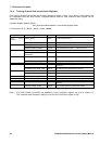
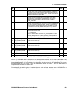
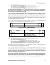
7.6.4 ACCUM_STATUS_B Register - Read Address offset 0x20C
ACCUM_STATUS_B is a register containing the state of twelve status bits sampled and latched on the active edge
of every ACCUM_INT (as for ACCUM_STATUS_A). They can also be sampled and latched on request, by
performing a write operation to STATUS.
Bit
No
Mnemonic Description
Reset
Value
R/W
15 DISCIP1_GLITCH The DISCIP_GLITCH bit will be set HIGH if a glitch to LOW has occurred
on the DISCIP pin since the last read of this register. It is cleared by
reading this ACCUM_STATUS_B register. This bit is reset by a hardware
master reset (NRESET at Low) but not by a software reset. The
minimum reliably detectable glitch width is 25ns.
0R