


7: 12-Channel Correlator
GP4020 GPS Baseband Processor Design Manual 75
7.6.17 CHx_CODE_PHASE Register - Read Offset <CHx_Control> + 0x04
CHx_CODE_PHASE_COUNTER Register - Write Offset <CHx_Control> + 0x04
MULTI_CODE_PHASE_COUNTER Register - Write Offset 0x180 + 0x04
ALL_CODE_PHASE_COUNTER Register - Write Offset 0x1C0 + 0x04
This register is primarily a Read Register (i.e. CHx_CODE_PHASE). However, if 'Test' mode has been selected by
setting TM_TEST (TEST_CONTROL[3]) to '1', the CHx_CODE_PHASE_COUNTER registers can be written to.
This is a test-mode, and is hence not normally required.
A read of CHx_CODE_PHASE[10:0] indicates the state of the Code Phase Counter, an 11-bit binary up-counter,
clocked by the Code generator clock. The Phase is expressed as a number of half code chips and ranges from 0 to
2046 chips. A reading of 2046 is very rare and can only occur if the TIC captures the Code phase just after the
counter reaches 2046 and before a DUMP from the C/A Code Generator resets it. DUMP also increments the
Epoch counter, so the meaning of a phase value of 2046 + the previous Epoch value is the same as a phase value
of (0 + the incremented Epoch value), and either is valid. If a TIC occurs during a Code Slew, the reading will be '0'
and that channel’s Measurement Data is of no use.
A write to CHx_CODE_PHASE_COUNTER[10:0] loads the written 11-bit value to Code Phase Counter for the
channel concerned. This is a Test Mode only, and is NOT required for normal use.
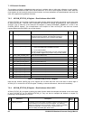
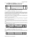
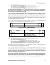
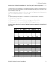
Bit
No.
Mnemonic Description Reset
Value
R/W
15:11
Not used
'0' when read. - R
10:0 CHx_CODE_PHASE [10:0] Bits 10:0 of the 11-bit Code Phase Count. 0x000 R
Table 7.20 CORR CHx_CODE_PHASE Register
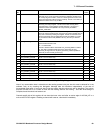
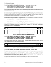
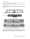
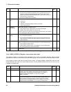
Bit
No.
Mnemonic Description Reset
Value
R/W
15:11
Not used
-W
10:0 CHx_CODE_PHASE _COUNTER[10:0] Bits 10:0 of the 11-bit Code Phase Count.
Write to the space only possible if
TEST_CONTROL[3] ('TM_TEST') set to '1'.
0x000 W
Table 7.21 CORR CHx_CODE_PHASE_COUNTER Register
7.6.18 CHx_CODE_SLEW Register - Read Address Offset <CHx_Control> + 0x00
CHx_CODE_SLEW_COUNTER Register
-
Write Address Offset <CHx_Accumulate> + 0x00
MULTI_CODE_SLEW_COUNTER Register - Write Address Offset 0x2D0 + 0x00
ALL_CODE_SLEW_COUNTER Register - Write Address Offset 0x2E0 + 0x00
This register space is primarily a Write Register (i.e. CHx_CODE_SLEW_COUNTER). However, the register can
also be read for test purposes, but does not have any system use.
A write to CHx_CODE_SLEW_COUNTER[10:0] gives an unsigned integer ranging from 0 to 2047. This represents
the number of code half chips to be slewed immediately after the next DUMP if in UPDATE mode or after the next
TIC, if in PRESET mode. Since there are only 2046 half chips in a GPS C/A code, a programmed value of 2047 is
equivalent to a programmed value of 1, but the next DUMP event will take place 1 ms later. In PRESET mode, the
slew timing is set only by TIC, which will also reset the code generator (no DUMP is needed). A non-zero slew must
always be programmed when using PRESET mode.
The CHx_CODE_SLEW register can be written to at any time. If two accesses have taken place before a DUMP in
UPDATE mode or before a TIC when in PRESET mode, the latest value will be used at the next slew operation.
During the time a slew process is being executed, any further write access to the CHx_CODE_SLEW register will
be stored until the following DUMP and then cause the transfer of this new value into the counter. This situation
may be avoided by synchronising the access with the associated CHx_NEW_ACCUM_DATA status bit.