


11: Memory Peripheral Controller
112 GP4020 GPS Baseband Processor Design Manual
Essentially, this equates to setting address 0xE000 8008 to a value of 0x3303 306E.
The MPC must be configured to address a 32-bit bus when accessing the Area 3 internal peripherals.
By using “Sub-memory access”, writes to the 12-channel correlator can be either 16-bit or 32-bit; 8-bit accesses are
NOT permitted. In the case of a 32-bit Write access, the 16MSBs of each access are ignored. In the case of a 32-
bit read access, the 16 MSBs of the data will be set to ‘0x0000’.
Writes to all other parts in Area 3 can be 8-, 16-, or 32-bit wide.
11.5 GP4020 Memory Area 4 Configuration
GP4020 Memory Area 4 is used to access the internal SRAM only in the GP4020, and NO other components. The
internal SRAM is configured as 2k x 32-bit data or 8k bytes and can be configured to have either 8-bit, 16-bit or 32-
bit data width. Also, the access time of the internal SRAM is high speed; only 6ns, and so can be accessed with 0-
wait-states for any Firefly MF1 BµILD CLK frequency setting.
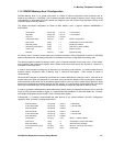
The default hard-wired configuration at Reset of MPC Memory Area 4 (register address 0xE000800C) is
0xFF000034:
Access Waits bits [31:28] = ‘0y1111’ = 15 wait states
Stop Waits bits [27:24] = ‘0y1111’ = 15 wait states
Reserved bits [23:8] = ‘0x0000’
Configuration Mode bits [7:6] = ‘0y00’ (Mode 0 configuration)
Wait Control bit [5] = ‘1’ (enable MPC control of Wait-states)
Read Only Status bit [4] = '1' (Read Only enabled)
Sub Memory Write Status bit [3] = ‘0’ (Sub memory writes disabled)
Access Type bit [2] = ‘1’ (Memory access)
Data Size bits [1:0] = '0y00' (Byte (8-bit) wide)
With the default settings shown above, an 8-bit SRAM can be read (but NOT written to), with 15 wait-states. One of
the first things to be done in software after boot will be to configure the MPC Configuration for Area 4 to more
optimal settings. As the internal SRAM is high-speed, 0-wait-state access can be used across any data width.
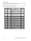
ALL the MPC registers are accessible at System Base Address 0xE000 8000.
Further details for the programming of the Memory Peripheral Controller can be found in Section 3 of the "Firefly
MF1 Core Design Manual" DM5003, available from Zarlink Semiconductor.