


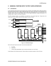
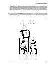
11: Memory Peripheral Controller
110 GP4020 GPS Baseband Processor Design Manual
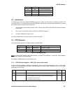
The default hard-wired configuration at Reset of MPC Memory Area 1 (register address 0xE000 8000) is 0xFF00
0035:
Access Waits bits [31:28] = ‘0y1111’ = 15 wait states
Stop Waits bits [27:24] = ‘0y1111’ = 15 wait states
Reserved bits [23:8] = ‘0x0000’
Configuration Mode bits [7:6] = ‘0y00’ (Mode 0 – See Note 1)
Wait Control bit [5] = ‘1’ (enable MPC control of Wait-states)
Read Only Status bit [4] = '1' (Read Only enabled)
Sub Memory Write Status bit [3] = ‘0’ (Sub memory writes disabled)
Access Type bit [2] = ‘1’ (Memory access – See Note 2)
Data Size bits [1:0] = '0y01' (Half Word (16-bit) wide)
Notes:
1) The Configuration Mode bits set the MPC Configuration for Area 1 to “Butterfly Mode” (Mode 0) by default.
Butterfly Mode does NOT give the same level of configuration flexibility as Standard Mode (Mode 1). (Refer to
details for this in the Memory Peripheral Controller section (Section 3) of the "Firefly MF1 Core Design Manual"
DM5003, available from Zarlink Semiconductor.)
2) Memory Access Type: signifies that a transaction may be constructed from multiple memory accesses; i.e.
operand size does not have to equal memory size.
3) ‘0x0000’ signifies a HEX number value of ‘0000’; ‘0y0000’ signifies a BINARY number value of ‘0000’.
With the default settings shown above, a 16-bit ROM can be read, with 15 wait-states. One of the first things to be
done in software after boot will be to configure the MPC Configuration for Area 1 to more optimal settings. Typically,
where a FLASH EPROM is used with NSCS[0], the access time tends to be quite slow (70ns to 100ns) but NOT
slow enough to need 15 wait-states. If the BµILD_CLK for the Firefly MF1 is set to 20MHz (default value), then the
period of each clock-cycle is 50ns. Therefore to access a 100ns FLASH EPROM, 2 access wait-states will need to
be introduced to guarantee that the data addressed in memory returns to the Firefly in time.
11.3 GP4020 Memory Area 2 Configuration
GP4020 Memory Area 2 is specified by addresses 0x2000 0000 through to 0x200F FFFF, and is typically used by
high-speed external 16-bit SRAM via chip-select line NSCS[1].
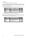
The default hard-wired configuration at Reset of MPC Memory Area 2 (register address 0xE000 8004) is 0xFF00
0034:
Access Waits bits [31:28] = ‘0y1111’ = 15 wait states
Stop Waits bits [27:24] = ‘0y1111’ = 15 wait states
Reserved bits [23:8] = ‘0x0000’
Configuration Mode bits [7:6] = ‘0y00’ (Mode 0 configuration)
Wait Control bit [5] = ‘1’ (enable MPC control of Wait-states)
Read Only Status bit [4] = '1' (Read Only enabled)
Sub Memory Write Status bit [3] = ‘0’ (Sub memory writes disabled)
Access Type bit [2] = ‘1’ (Memory access)
Data Size bits [1:0] = '0y00' (Byte (8-bit) wide)
With the default settings shown above, an 8-bit SRAM can be read (but NOT written to), with 15 wait-states. One of
the first things to be done in software after boot will be to configure the MPC Configuration for Area 2 to more
optimal settings. Typically, where a SRAM is used with NSCS[1], the access time tends to be fast (10ns to 20ns). If
the BµILD_CLK for the Firefly MF1 is set to 20MHz (default value), then the period of each clock-cycle is 50ns.
Therefore, to access a 10ns FLASH EPROM, no access wait-states are required.