


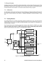
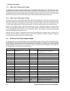
7: 12-Channel Correlator
60 GP4020 GPS Baseband Processor Design Manual
iv. Release the relevant CHx_RSTB bits of the RESET_CONTROL register to make the channel active.
When the code clock is inhibited (to slew the code phase), the Integrate and Dump module is held at reset. It will
start to accumulate correlation results only after the slew operation is completed.
A search for a satellite on more than one channel may be performed using the MULTI channel addresses and
different code slew values as appropriate.
7.4.5 Reading the Accumulated Data
At each DUMP, the corresponding CHx_NEW_ACCUM_DATA status bit is set in the ACCUM_STATUS_A register.
The status register, together with all accumulation registers (CHx_I_TRACK, CHx_Q_TRACK, CHx_I_PROMPT,
CHx_Q_PROMPT) are mapped into consecutive addresses. These can be read as a consecutive block, if required,
after every ACCUM_INT interrupt. Alternatively, the Status Registers may be polled. The Accumulation registers
are not overwrite-protected; therefore the system must respond quickly when new data becomes available.
Whether or not it is necessary to process the accumulation at every DUMP is dependent upon the application. The
order of reading them is optional, but ideally, the CHx_Q_PROMPT register should be read last, because this
resets the CHx_NEW_ACCUM_DATA bit. The CHx_MISSED_ACCUM bits in the ACCUM_STATUS_B register
indicate that new accumulated data has been missed. These can only be cleared by a write to
CHx_ACCUM_RESET or by deactivating the channel.
7.4.6 Search on Other Code Phases
When it is desired to correlate on the next code phase, such as one whole chip later, the CODE_SLEW has to be
programmed with a value of 2 (the units are half code chips). The slew will occur on the next DUMP. The effect of
CODE_SLEW is relative to the current code phase. To repeat a CODE_SLEW, the register needs to be written to
again even if the same size slew is required.
Once the signal has been detected (correlation threshold exceeded), the code and carrier tracking loops can be
closed.
The tracking loop parameters must be tailored in the software to suit the application.
7.4.7 Data Bit Synchronisation
The data bit synchronisation algorithm should find the data bit transition instant. The processor calculates the
present one-millisecond epoch and programs this value into the 1MS_EPOCH counter. Ideally, epoch counter
accesses should occur following the reading of the accumulation register at each DUMP.
Alternatively, the epoch counters can be left free–running and the offset can be added by the software each time it
reads the epoch registers. Note that if the integration is performed across bit boundaries, the integration result can
be very small.
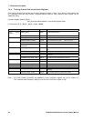
7.4.8 Reading the Measurement Data
At each TIC, the measurement data is latched in the Measurement Data registers (CHx_EPOCH,
CHx_CODE_PHASE, CHx_CARRIER_DCO_PHASE, CHx_CARRIER_CYCLE_HIGH,
CHx_CARRIER_CYCLE_LOW, and CHx_CODE_DCO_PHASE).
The ACCUM_STATUS_B or MEAS_STATUS_A register must be polled at a rate greater than the TIC rate (to see if
a TIC has occurred), otherwise measurement data will be lost. The ACCUM_INT or MEAS_INT events can be used
to instigate this operation. The reading of measurement data can be either interrupt driven or polled.
For the interrupt driven method the microprocessor reads the ACCUM_STATUS_B or MEAS_STATUS_A register
after each MEAS_INT, and if the TIC bit is set, subsequently reads the Measurement data.