


15: 1PPS Timemark Generator
GP4020 GPS Baseband Processor Design Manual 165
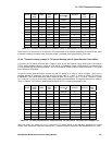
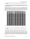
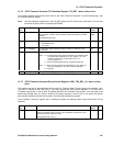
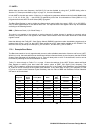
15.7.2 1PPS Timemark Generator TIC Retention Register- TIC_RET - Memory Offset 0x012
This register combines control and monitor lines for the 1PPS Timemark Generator TIC period slewing logic, with
an 8-bit data retention register.
Note: The Data Retention register bits in the TIC_RET register are NOT reset by any reset event. This can only
be cleared by writing ‘0x00’ or powering off GP4020.
Bit
No.
Mnemonic Description Reset
Value
R/W
15:8 RETEN[7:0] Data Retention Register. An 8bit store location which is NOT reset by any
control signals. Could be used to indicate a total power failure in the GPS
Receiver.
Most Significant Bit = Bit 7
Not
Reset
R/W
7 TIC_TIME Toggle signal on TIMEMARK/TIC output pin (pin 69 (100-pin package)):
'0' = TIMEMARK output
'1' = TIC output
0R/W
6:4 TIC_CORR[2:0] TIC Correction (delay) required for each TIC Event, in units of M_CLK
cycles (25ns).
000 R/W
3 ADJ_TIC TIC Period Extension Status / Control bit
Read: '1' = TIC period skew Phase_offset calculation has overflowed. Next
TIC period will be extended if TIC_INT_EN[1:0] = '01, and
should be extended by a write to ADJ_TIC of '1', if
TIC_INT_EN[1] = '1'].
'0' = next TIC period should NOT be / will NOT be extended
Write: '1' = causes next TIC period to be extended (if TIC_INT_EN[1] (in
PER_STAT register)) is set. (Also clears set read bit).
'0' = No effect.
0R/W
2:0 PHASE_OFF[2:0] Current value of Phase offset in Phase-offset calculation. 000 R
Table 15.11 1PPS Timemark TIC_RET Register
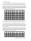
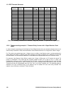
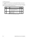
15.7.3 1PPS Timemark Generator Delay Counter Register (LSB) - TIM_DEL_LO - Memory Offset
0x014
This register sets the 16 least significant bits for the 22-bit Timemark Delay Counter down-count initialised value,
TIM_DEL, in conjunction with TIM_DEL_HI. The value signifies the delay required between a TIC event and a
Timemark output pulse, in units of 25ns. The default period for the Timemark output pulse is 1ms, and needs to be
added onto the total delay (i.e. add on 40,000) to any delay required in order to give a 1ms pulse. Only values
above 40,000 (0x9C40) are valid in this register. All values below 40,000 are ignored.
This is primarily a write-only register, but on reading the register, the settings made by the previous Write can be
observed.
Bit
No.
Mnemonic Description Reset
Value
R/W
15:0 TIM_DEL[15:0] Set LSBs of number of M_CLK clock cycles by which TIC should be delayed
before a Timemark Pulse is produced, and completed. Pulse period of 1ms
(40,000) should be added onto delay.
Most Significant Bit = Bit 15.
0x9C40 R/W
Table 15.12 1PPS Timemark TIM_DEL_LO Register