


6: BSIO Interface
38 GP4020 GPS Baseband Processor Design Manual
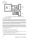
SCLK
SDIO
DATA OUT
SDIO
DATA IN
SCLK
SDIO
DATA OUT
SDIO
DATA IN
SCLK
SDIO
DATA OUT
SDIO
DATA IN
WRPOL = 1, RDPOL = 0, CYCDELAY = 0
SCLK
SDIO
DATA OUT
SDIO
DATA IN
WRPOL = 1, RDPOL = 0, CYCDELAY = 1WRPOL = 0, RDPOL = 0, CYCDELAY = 1
WRPOL = 0, RDPOL = 0, CYCDELAY = 0
SCLK
SDIO
DATA OUT
SDIO
DATA IN
SCLK
SDIO
DATA OUT
SDIO
DATA IN
SCLK
SDIO
DATA OUT
SDIO
DATA IN
WRPOL = 1, RDPOL = 1, CYCDELAY = 0
SCLK
SDIO
DATA OUT
SDIO
DATA IN
WRPOL = 1, RDPOL = 1, CYCDELAY = 1WRPOL = 0, RDPOL = 1, CYCDELAY = 1
WRPOL = 0, RDPOL = 1, CYCDELAY = 0
TXDn
RXD0
TXDn
TXDn
TXDn
RXD0
RXD0
RXD0
TXDnTXDn
TXDnTXDn
RXD0 RXD0
RXD0
RXD0
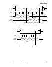
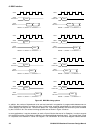
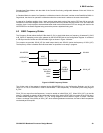
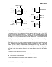
Figure 6.5 BSIO Bit timing options
In addition, the number of bytes/words to be sent and received in an operation is programmable between zero to
1023. Bit transfers will occur, on either the rising or falling edge, specified independently for read and write cycles
via the RDPOL and WRPOL bits. This has the option of a 1-cycle delay between write and read cycles controlled
by the CYCDELAY bit. The various bit timings possible are as shown in Figure 6.5 above.
In some applications, it may be necessary to send a Control Word at the start of an Operation. In order to support
this the BSIO provides a Page Mode in addition to the Standard Mode described above. The Control Word is held
in a separate 32-bit Parallel In / Serial Out Register. The CWORDSEL bit in the Mode Register selects between