


20: Input / Output pin Characteristics
190 GP4020 GPS Baseband Processor Design Manual
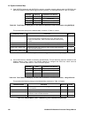
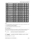
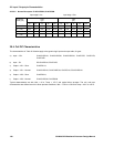
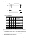
20.3.2.2 Normal N outputs: CLAIO1HD03N, CLAOP03N.
Input edge 0.1ns Input edge 1.5ns
Switching
Delay (ns)
Load
(pF)
Load
(pF)
10 20 40 80 150 10 20 40 80 150
D → OP ↑
5.82 6.99 8.89 11.75 15.76 5.55 6.72 8.62 11.48 15.49
D → OP ↓
5.55 6.75 8.60 11.18 14.48 6.37 7.56 9.42 11.99 15.30
T → OP ↑
6.10 7.27 9.18 12.05 16.06 6.91 8.08 9.99 12.86 16.87
T → OP ↓
5.49 6.66 8.49 11.04 14.33 6.30 7.47 9.30 11.85 15.15
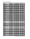
Table 20.8 X03 Normal N 3.3V Output delays
20.4 Cell DC Characteristics
The characteristics in Table 20.9 below apply to the generic logic input and output cells, of types:
a) Input - 3.3V: CLAIO1HD01N, CLAIO1HD03N, CLAIO1NR01N, CLAIP1GD, CLAIP1GU,
CLAIP1NR
b) Input – 5V: SCJIO1NR01N, SCJIP1NR,
c) Output – X01 – Slow: CLAOP01L1,
d) Output – X01 – Normal: CLAIO1HD01N, CLAIO1NR01N, CLAOP01N, SCJIO1NR01N
e) Output – X03 – Slow: CLAOP03L1,
f) Output – X03 – Normal: CLAIO1HD03N, CLAOP03N
Typical characteristics are with Vdd = +3.3v, Temp = +27°C and typical silicon process. The min. and max.
characteristics are defined over ALL silicon process conditions, Vdd = +3.0V to +3.6V and Temp = -40°C to +85°C.