


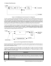
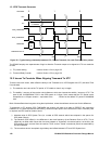

14: System Clock Generator
148 GP4020 GPS Baseband Processor Design Manual
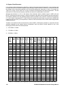
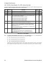
14.6.2 SCG PLL Control Register - PLL_CNTL - Memory Offset 0x00A
A write to this register stores logic values which set or reset input control lines to the PLL within the System Clock
Generator. A read of this register shows the status of these functions.
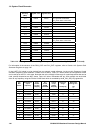
Bit
No.
Mnemonic Description Reset
Value
R/W
15 TM2
Reserved for PLL Test, in UIM_TEST mode only 0 Note 1
14 TM1
Reserved for PLL Test, in UIM_TEST mode only 0 Note 1
13 SG1
Reserved for PLL Test, in UIM_TEST mode only 0 Note 1
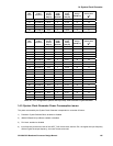
12:11 VCOD[1:0] PLL VCO Output Frequency Range selection pin. This input determines which
of the 4 frequency ranges are selected.
'00' operates the VCO between 80MHz and 250MHz;
'01' operates the VCO between 40MHz and 125MHz;
'10' operates the VCO between 20MHz and 63MHz;
'11' operates the VCO between 10MHz and 32MHz
11 R/W
10:6 CHP[4:0]
PLL Charge Pump setting. Values determined by numbers in
Table 14.2 on
page 142, Table 14.3 on page 143 and Table 14.4 on page 144.
00101 R/W
5:1 DIV[4:0] PLL Clock Multiplication Factor. Programmable divider programming bits used
for setting up the PLL in clock multiplication mode. These inputs are binary
weighted to give divider settings from 2 to 25. The binary value of ‘n’ will give a
divider setting of N = n+2.
For clock synchronisation (divide by 1) set SYNCEN to a ‘1’ and DIV0-4 all to a
‘1’ (to minimise power consumption).
11111 R/W
0 SYNCEN PLL Clock Synchronisation Enable. Allows PLL to produce an output frequency
at multiplication factor of 1.
‘1’ = enable Clock Synchronisation mode (i.e. Multiplication fixed at 1)
‘0’ = enable Clock Multiplication mode (i.e. Programmable Multiplication
between 2 and 25)
1R/W
Table 14.8 PLL_CNTL Register
Note 1: In 'UIM_test_mode' (selected by TEST (pin 67) = "1", and TESTMODE (pin 74) = "1"), if the address input,
chip select and write enable are doing a "write" to the 'PLL_CNTL' register:
• SG1 is controlled directly by bit 13 of the data bus;
• TM1 is controlled directly by bit 14 of the data bus;
• TM2 is controlled directly by bit 15 of the data bus;
These bits [15:13] are NOT latched in the PLL_CNTL register. All the other bits in the PLL_CNTL register,
will be updated at the negative edge of UART_CLK, while the write to the PLL_CNTL address continues).