


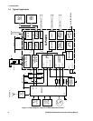
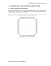
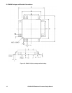
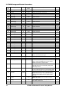
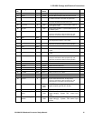
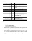
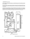

2: GP4020 Package and Electrical Connections
14 GP4020 GPS Baseband Processor Design Manual
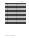
Pin
No.
Signal Name Type Circuit
Block
Description Notes
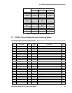
24 SDATA[7] I/O MPC System Data bit 7 1
25 NSOE I/O MPC System Output Enable - Active Low 1
26 NSWE[1] I/O MPC System Write Enable bit 1 - Active Low 1
27 NSWE[0] I/O MPC System Write Enable bit 0 - Active Low 1
28 SDATA[8] I/O MPC System Data bit 8 1
29 SDATA[9] I/O MPC System Data bit 9 1
30 VDD PWR
31 SDATA[10] I/O MPC System Data bit 10 1
32 SDATA[11] I/O MPC System Data bit 11 1
33 GND PWR
34 SDATA[12] I/O MPC System Data bit 12 1
35 SDATA[13] I/O MPC System Data bit 13 1
36 SDATA[14] I/O MPC System Data bit 14 1
37 SDATA[15] I/O MPC System Data bit 15 1
38 SADD[18] I/O MPC System Address bit 18
39 SADD[17] I/O MPC System Address bit 17
40 SADD[16] I/O MPC System Address bit 16
41 GND PWR
42 SADD[15] I/O MPC System Address bit 15
43 SADD[14] I/O MPC System Address bit 14
44 VDD PWR
45 SADD[13] I/O MPC System Address bit 13
46 SADD[12] I/O MPC System Address bit 12
47 SADD[11] I/O MPC System Address bit 11
48 SADD[10] I/O MPC System Address bit 10
49 SADD[9] I/O MPC System Address bit 9
50 SADD[8] I/O MPC System Address bit 8
51 SWAIT I MPC System Wait input - allows wait-states to be inserted
into the current Firefly clock cycle.
52 NSUB O MPC System Upper Byte - Active Low 1,2
53 IEXTINT2 I INTC Interrupt source 2 input (for external interrupts)
54 MULTI_FNIO I/O PCL Multi-function Input / Output.
Used to set Boot Up ROM area, and source either
100kHz square wave or System Clock
55 DISCIO I/O PCL Discrete Input / Output
Used either as input or to source RF_Power_Down
control signal or TIC.
3
56 RF_PLL_LOCK I INTC / PCL
PLL Lock Indicator input from RF section. When High
this signal indicates that the PLL within the RF section
is in lock and the master-clock inputs have stabilised.
57 A1VDD PWR VDD Supply for CLK_T & CLK_I input block in the
System Clock Generator. This pin should be well de-
coupled to pin 60 (GND) to ensure optimum noise
immunity.
58 CLK_T I SCG Master Clock (M_CLK) Input from RF Front-end -
40MHz 100mV rms.
4
59 CLK_I I SCG Inverted Master Clock (M_CLK) Input from RF Front-
end - 40MHz 100mV rms.
4
60 GND PWR