


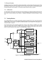
7: 12-Channel Correlator
GP4020 GPS Baseband Processor Design Manual 59
milliseconds, an improved first guess for local time could include an allowance for this delay to reduce the iteration
time later.
By using the data to time-tag the TIC, along with the values of the Epoch counter, the Code generator phase, and
the Code clock phase it is possible to measure the time of the SV signal in local apparent time. This gives the value
of t
1
needed for the pseudo-range measurement. The pseudorange can now be computed as t
1
-t
2
.
The error present in the time setting is the initial value of the user clock bias, with an allowance for the various
counter phases. Once a Navigation Solution has been found the clock error is precisely known and may be used for
future pseudorange calculations. Due to the receiver clock drifting with time, the clock-bias changes with time, and
this must be tracked by the Navigation software.
7.4 Controlling the 12 Channel Correlator
The following section describes typical methods for controlling the 12-channel correlator block in the GP4020.
These include signal acquisition tracking and carrier phase measurement.
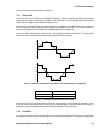
7.4.1 Search Operation
To perform signal acquisition, the carrier frequency and code phase space needs to be searched until the signal is
detected. The maximum carrier frequency excursion from its nominal value is defined by the maximum carrier
Doppler shift plus the maximum receiver clock error. The maximum code phase is defined by the (fixed) code
length. Typically, all code phases will be searched at a given carrier frequency before advancing to the next carrier
frequency bin and repeating the code phase search.
7.4.2 Carrier DCO Programming
The CHx_CARRIER_DCO_INCR_HIGH (or X_DCO _INCR_HIGH), and CHx_CARRIER_DCO_INCR_LOW
registers are programmed in sequence with the relevant data according to the frequency bin being searched. It is
always necessary to write to both the _HIGH and _LOW registers. Carrier DCO programming will become effective
as soon as the channel is released (made active). If the channel is already active, writes to
CHx_CARRIER_DCO_INCR_LOW are effective immediately. (A small delay of up to 175ns will occur, to allow
synchronisation of the processor write operation to the chip operation.)
7.4.3 Code DCO Programming
The CHx_CODE_DCO_INCR_HIGH (or X_DCO_INCR_HIGH), and the CHx_CODE_DCO_INCR_LOW registers
are programmed in sequence with the relevant data according to the estimated code frequency offset. It is always
necessary to write to both _HIGH and _LOW registers. Code DCO programming will become effective as soon as
the channel is released (made active). If the channel is already active, writes to CHx_CODE_DCO_INCR_LOW are
effective immediately. (A small delay of up to 175ns will occur to allow synchronisation of the processor write
operation to the chip operation).
7.4.4 Code Generator Programming
For each channel, the CHx_SATCNTL register is programmed as follows:
i. Set the TRACK_SEL bits to set the Tracking arm code to either early or late (with respect to the Prompt arm).
ii. Set the G2_LOAD bits to select the required PRN code.
iii. Program the CHx_CODE_SLEW register with the desired code phase offset. The slew operation will become
effective upon CHx_RSTB release. The first DUMP will generate accumulated data for the channel and set
the associated CHx_NEW_ACCUM_DATA status bit.