


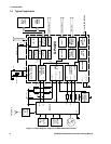
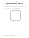
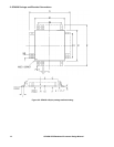
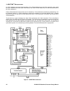

2: GP4020 Package and Electrical Connections
GP4020 GPS Baseband Processor Design Manual 15
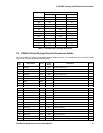
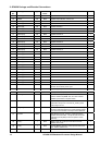
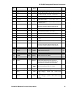
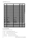
Pin
No.
Signal Name Type Circuit
Block
Description Notes
61 SIGN0 I CORR Sampled Sign (polarity) data from RF Front-end
62 MAG0 I CORR Sampled Mag (amplitude) data from RF Front-end
63 SAMPCLK O CORR Sample Clock output to the RF front end. Provides a
5.714MHz clock with a 4:3 mark–to–space ratio.
64 POWER_GOOD I PCL Power Monitor input. High for normal operation. Low
forces the GP4020 into Power Down mode.
65 PR_XOUT O SCG System Clock Oscillator - crystal oscillator output for
10 to 16MHz crystal.
66 PR_XIN I SCG System Clock Oscillator - crystal oscillator input for 10
to 16MHz crystal.
67 TEST I Test Select Pin. Used with TESTMODE (Pin 74).
This pin is reserved for TEST purposes only and
should be connected to GND in normal operation.
5
68 VDD PWR
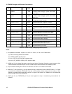
69 TIMEMARK / TIC O 1PPS Timemark output. This pin can be used to produce a
UTC-aligned 1PPS output, or TIC output
70 IDDQTEST I
This pin is reserved for TEST purposes only and
should be connected to GND in normal operation
71 GND PWR
72 RTC_XIN I RTC Real-time Clock Crystal Oscillator input for 32kHz
crystal.
73 RTC_XOUT O RTC
Real-time Clock Crystal Oscillator output for 32kHz
crystal
74 TESTMODE I Test-mode Select Pin. Used with TEST (Pin 67).
This pin is reserved for TEST purposes only and
should be connected to GND in normal operation.
5
75 NSRESET I PCL System Reset input
76 U2TXD O UART2 UART 2 Transmit data output.
77 U2RXD I UART2 UART 2 Receive data input. 3
78 U1TXD O UART1 UART 1 Transmit data output.
79 U1RXD I UART1 UART 1 Receive data input. 3
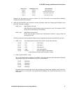
80 PLLGND PWR SCG PLL GND connection for PLL Block
81 PLLVDD PWR SCG PLL VDD connection for PLL Block
82 GND PWR
83 PLLAT1 O SCG PLL System Clock Generator PLL Analog Test IO.
This pin is reserved for TEST purposes only and
should be NOT connected in normal operation
84 NICE I JTAG /
SSM
MUX
ARM7TDMI operating mode and JTAG / SSM
signal multiplex (pins 86, 87, 88, 89).
6
85 VDD PWR
86 TCK / bdiag[0] /
XReq
I/O JTAG /
SSM
JTAG Test Clock / SSM Diagnostic broadcast
output bdiag[0] / System Test control input
XReq
6
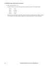
87 TDI / bdiag[1] /
XWrite
I/O JTAG /
SSM
JTAG Test Data In / SSM Diagnostic broadcast
output bdiag[1] / System Test control input
XWrite
6