


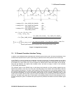
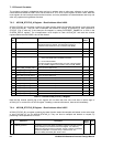
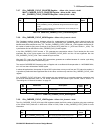

7: 12-Channel Correlator
GP4020 GPS Baseband Processor Design Manual 67
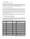
Address Offset Register Direction Function
CHx_
Accumulate
+ 0x00 I_TRACK READ Integrate and Dump Values for I tracking arm in
correlator channel X.
CODE_SLEW
_COUNTER
WRITE Sets number of code half-chips to slew the C/A
code generator at next DUMP event.
+ 0x04 Q_TRACK READ Integrate and Dump Values for Q tracking arm in
correlator channel X.
ACCUM_RESET WRITE Reset ACCUM_STATUS_X registers.
+ 0x08 I_PROMPT READ Integrate and Dump Values for I prompt arm in
correlator channel X.
not used
WRITE
+ 0x0C Q_PROMPT READ
Integrate and Dump Values for Q prompt arm in
correlator channel X.
CODE_DCO
_PRESET_ PHASE
WRITE 8 MSBs of CODE_DCO phase to be loaded at
next TIC event, in PRESET mode.
Table 7.4 CORR Tracking Channel Data Accumulation Registers Map
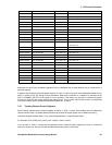
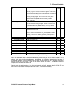
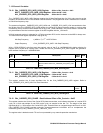
Address
Offset
Register Direction Function
0x200 ACCUM_STATUS_C READ Indicates either "Early" or "Late" codes, on each
correlator channel.
STATUS WRITE Latches data on ALL ACCUM_STATUS registers
0x204 MEAS_STATUS_A READ Indicates if Measurement data has been missed, on
each correlator channel.
not used
WRITE
0x208 ACCUM_STATUS_A READ
Indicates if new Accumulation data is available on each
correlator channel.
not used
WRITE
0x20C ACCUM_STATUS_B READ Indicates if new Accumulation data has been missed,
on each correlator channel.
not used
WRITE
Table 7.5 CORR Tracking Channel Status Registers Map
Apart from the Code and Carrier DCO increment values, all data transfers are only 16-bits wide. Writes to the Code
and Carrier DCO’s are 32-bit data transfers. The _HIGH word should be written first and will be retained in the 16- to
32-bit interface until the _LOW word is written. The _LOW word write must occur as the next write to the chip. All 32-
bits will then be transferred into the DCO increment register. Data is written to an input buffer in the 16- to 32-bit
interface and will be transferred to its destination register during the next full cycle of the 7 (or 6) phase clock. Write
cycles should therefore have a period of at least 300ns. The X_DCO_INCR_HIGH may be used to write the high bits of
the increment number to any or all DCO’s as an alternative to using the CHx_CODE / CARRIER_DCO_INCR– _HIGH
addresses. By using this address, there is no need to wait 300ns before writing the _LOW part. For further information,
refer to Section 7.5 "12 Channel Correlator Interface Timing" on page 63.
The bit assignments for the Correlator registers are given below, but two write–only registers do not have any data bits,
these are:
1) A write to the CHx_ACCUM_RESET register (irrespective of what data is written) will reset the
ACCUM_STATUS_A, ACCUM_STATUS_B, and ACCUM_STATUS_C registers for that channel.
2) A write to the STATUS register (irrespective of what data is written) will latch the state of the various status
flags into ACCUM_STATUS_A, ACCUM_STATUS_B, ACCUM_STATUS_C registers for all channels. This
allows polling based, rather than Interrupt driven tracking scheme.