


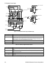
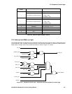
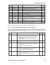
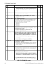
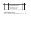

12: Peripheral Control Logic
126 GP4020 GPS Baseband Processor Design Manual
Bit
No.
Mnemonic Description Reset
Value
R/W
10 RF_SLEEP
'1' = Disable 40MHz low-level differential input in System Clock Generator,
and apply an active High power-down signal to the RF Front-end (via
DISCIO (pin 55 (100-pin package)), if so configured (ref. IO_REV
register). Can be re-enabled by a wake-up event.
'0' = no effect
0R/W
9 PLL_SLEEP
'1' = Disable and reset the PLL in System Clock Generator. Can be re-
enabled by a wake-up event. (See Note)
'0' = no effect
0R/W
8 F_SLEEP
'1' = Disable the Firefly MF1 system clock (B
µILD_CLK). Can be re-
enabled by a wake-up event.
'0' = no effect
0R/W
7:6 B_CLK_SEL[1:0] UART_CLK divider block selector.
Allows selection of different output division ratios for the B_CLK signal, to
allow small resolution changes in B_CLK frequency, if required. The
divider ratio is set to divide by 1, in the reset condition.
'00' = divide by 1 (i.e. through connection)
'01' = divide by 2
'10' = divide by 4
'11' = divide by 8
00 R/W
5 PLL_BYP
PLL Bypass connection. Allows input signal to PLL to appear at input to
B_CLK divider block, effectively removing PLL from signal path. The PLL
is bypassed in the reset condition.
'1' = Enable PLL bypass, remove PLL from the signal path.
'0' = Disable PLL bypass, connect PLL.
1R/W
4:3 PLL_IN_SEL[1:0]
(See Note)
PLL Input (& PLL Bypass) signal selector. Allows either divided down
versions of the M_CLK signal (20.0MHz or 10.0MHz) or a signal from the
Processor Crystal Oscillator (10.0MHz to 16.0MHz) to be applied to the
PLL CLKINB input as a PLL reference signal. M_CLK / 2 is applied to the
PLL CLKINB input in the reset condition.
'0x' = connect the output from the Processor Crystal Oscillator to PLL
CLKINB input
'10' = connect M_CLK / 2 (=20MHz) to PLL CLKINB input
'11' = connect M_CLK / 4 (=10.0MHz) to PLL CLKINB input
10 R/W
2 PLL_PD PLL Power Down. PLL is Disabled in the reset Condition
'1' = disable the PLL immediately.
'0' = Enable the PLL after a wait period of approx. 183
µs (6 * 32kHz clock
cycles, determined by the Real Time Clock block). This allows the
CLKINB to stabilise.
1R/W
1 PRX_EN Enable Processor Crystal Oscillator block..
'1' = Enable the Processor Crystal Oscillator; start up time in 10ms typical
'0' = disable the Processor Crystal Oscillator. Only to be done if B_CLK is
derived directly from M_CLK.
1R/W
0 RF_PD Power Down RF Front-end and 40MHz Low Level Differential Block.
Blocks are powered Up in the Reset Condition.
'1' = disable the Differential Block and apply an active High power-down
signal to the RF Front-end (via DISCIO (pin 55 (100-pin package)), if
so configured (ref. IO_REV register). Should only be used if B_CLK is
derived from the Processor Crystal Oscillator.
'0' = re-enable the Differential Block and apply an active Low power-on
signal to the RF Front-end (via DISCIO (pin 55 (100-pin package)), if
so configured (ref. IO_REV register).
0R/W
Table 12.5 PCL POW_CNTL Register