


15: 1PPS Timemark Generator
164 GP4020 GPS Baseband Processor Design Manual
15.7 1PPS Timemark Generator Registers
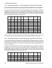
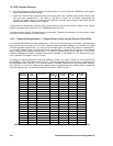
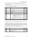
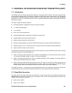
The Timemark Generator uses four registers. These registers are addressable in the same part of the memory
map as the Peripheral Control Logic Block - Root address 0x4010 1000.
Address
Offset
Register Direction Function
0x010 PER_STAT Read/Write Used to set interrupts and Resets for the WHOLE
GP4020 chip. Primarily used in the Peripheral Control
Logic (PCL) block. Bits 14 and 15 used to configure the
Tic Period Slew Overflow controller.
0x012 TIC_RET Read/Write
TIC Retention register, used to configure the TIC Period
slewing logic, and access a data retention register.
0x014 TIM_DEL_LO Read/Write Timemark Delay Down-Counter setting bits - 15 Least
Significant bits
0x016 TIM_DEL_HI Read/Write Timemark Delay Down-Counter setting bits - 6 Most
Significant bits
Also 2 control bits
Table 15.9 1PPS Timemark Generator Register Map
All registers are addressable as 32-bit locations only, but can use sub-memory access. This is particularly useful for
the TIM_DEL_HI register, which is only 8-bits wide.
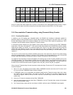
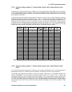
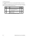
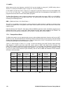
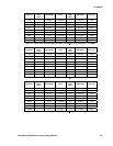
15.7.1 1PPS Timemark STATUS Register - PER_STAT - Memory Offset 0x010
This register is used to control Interrupts and Resets within the GP4020, and most of the controls are handled
within the PCL block. The 1PPS Timemark generator uses 2-bits from this register as write bits for the Control of
the Timemark Overflow Control block. This is primarily a write-only register, but on reading the register, the settings
made by the previous Write can be observed.
Bit
No.
Mnemonic Description Reset
Value
R/W
15:14 TIC_INT_EN[1:0]
Control of the TIC_INT signal interrupt within the Overflow Control Block of
the TIC Period slewing logic.
'00' = Disable TIC_INT and RELOAD_TIC signals
'01' = Enable TIC_INT and RELOAD_TIC signals. TIC_INT and
RELOAD_TIC signals generated each time Modulo 7 adder overflows
- automatic TIC period extension occurs. ADJ_TIC bit (TIC_RET
Register) set also.
'10' = Enable TIC_INT and RELOAD_TIC signals. TIC_INT and ADJ_TIC bit
(TIC_RET Register) set each time Modulo 7 adder overflows. A Read
of ADJ_TIC and subsequent write to ADJ_TIC will set RELOAD_TIC
and cause a TIC period extension. If ADJ_TIC not written to, no
RELOAD_TIC generated and TIC will not be extended.
'11' = Enable TIC_INT and RELOAD_TIC signals. TIC_INT set for every TIC,
irrespective of adder overflow state. ADJ_TIC bit (TIC_RET Register)
set each time Modulo 7 adder overflows. A Read of ADJ_TIC and
subsequent write to ADJ_TIC will set RELOAD_TIC and cause a TIC
period extension. If ADJ_TIC not written to, no RELOAD_TIC
generated and TIC will not be extended.
00 R/W
13:0
Reserved for use by Peripheral Control Logic (PCL)
Table 15.10 1PPS Timemark PER_STAT Register