


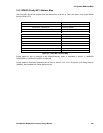
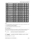
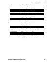
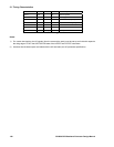

20: Input / Output pin Characteristics
GP4020 GPS Baseband Processor Design Manual 191
Parameter Cell
Type
Min Typ Max Unit Conditions
Input Leakage All IP -1 +1
µA
No Pull Up/Down, VDD = 3.6V
Output (Tristate) Leakage All OP 1
µA
No Pull Up/Down, VDD = 3.6V
Input Capacitance All IP 5 pF Not including Package
Output Capacitance All OP 5 pF Not including Package
Weak Pull-up Current GU IP -30
µA
Input at 0V
Weak Pull-down Current GD IP 30
µA
Input at VDD
Input Hold-Up Current HD IP -24
µA
Vin = 55% of VDD
Input Hold-Down Current HD IP 19
µA
Vin = 30% of VDD
Input Hold Threshold HD IP 1.48 V VDD = 3.3V
Low Input Level – CMOS VIL All IP 0.3
Vdd
V 3.0<VDD<3.6
High Input Level – CMOS VIH All IP 0.7
Vdd
V 3.0<VDD<3.6
Low Output Level – CMOS VOL All OP 0.4 V 3.0<VDD<3.6
High Output Level – CMOS VOH All OP 2.4 V 3.0<VDD<3.6
Low Output Current IOL X01 OP 2 mA
High Output Current IOH X01 OP 2 mA
Low Output Current IOL X03 OP 6 mA
High Output Current IOH X03 OP 6 mA
Table 20.9 Input & Output Cell DC Characteristics