


7: 12-Channel Correlator
74 GP4020 GPS Baseband Processor Design Manual
7.6.14 CHx_CODE_DCO_INCR_LOW Register - Offset <CHx_Control> + 0x18
MULTI_CODE_DCO_INCR_LOW Register - Offset 0x180 + 0x18
ALL_CODE_DCO_INCR_LOW Register - Offset 0x1C0 + 0x18
This register contains the 16 least significant bits for the CHx_CARRIER_DCO_INCR register. Refer to
"CHx_CODE_DCO_INCR_HIGH" for more information.
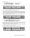
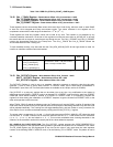
Bit
No.
Mnemonic Description Reset
Value
R/W
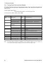
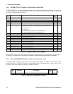
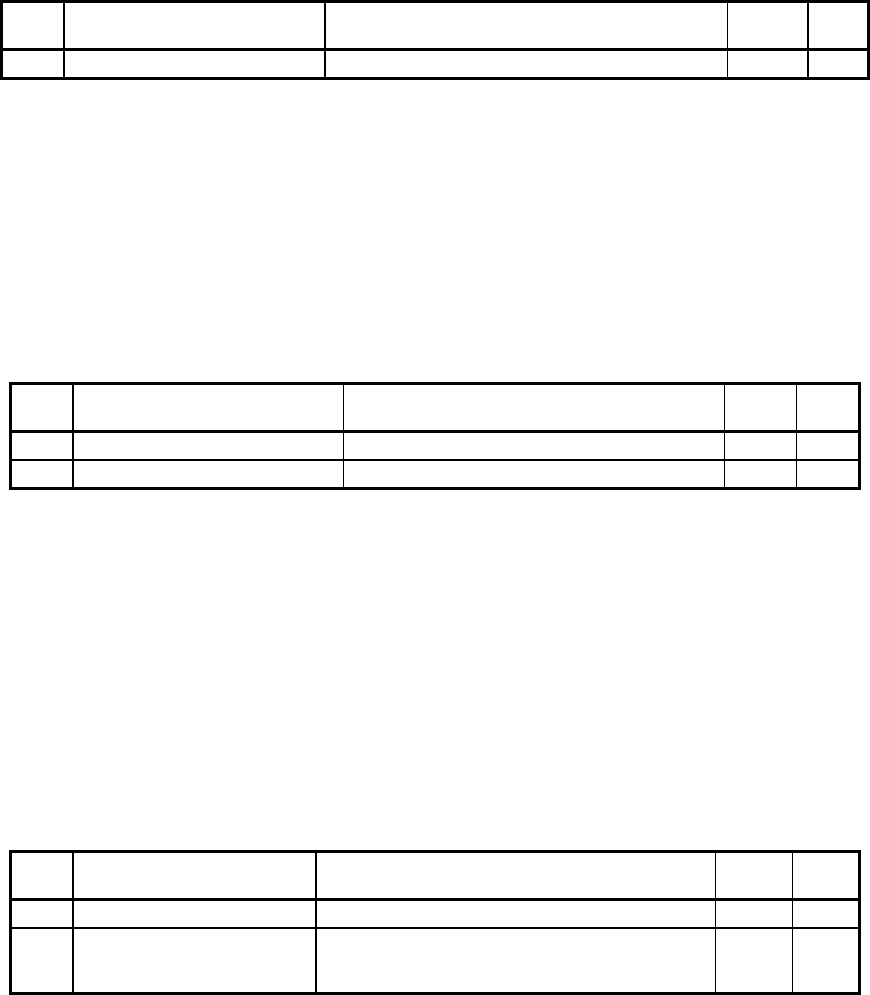
15:0 CHx_CODE_DCO_INCR [15:0] Bits 15:0 of the 25-bit Code DCO Increment Register 0x0000 W
Table 7.17 CORR CHx_CODE_DCO_INCR_LOW Register
7.6.15 CHx_CODE_DCO_PHASE Register - Offset <CHx_Control> + 0x14
This register contains the 10-bits of the Code DCO phase accumulator, and indicates the phase of a Code DCO
cycle, as a 10-bit sub-multiple of one Code DCO cycle, as sampled at the last TIC. The weight of the least
significant bit is 2π / 1024 radians of a Code DCO cycle, 2π being half of a code chip. Therefore, the pseudorange
resolution is 1/2048 of a chip, (equivalent to 0.15 metre or 0.5ns). These bits form an unsigned integer valid from 0
to 1023. CHx_CODE_DCO_PHASE provides sub-cycle phase-measurement information and so complements the
information given by CHx_CODE_CYCLE_HIGH and _LOW.
The register value is latched on each TIC and is not protected by any overwrite protection mechanism.
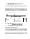
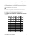
Bit
No.
Mnemonic Description Reset
Value
R/W
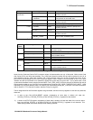
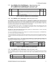
15:10
Not used
'0' when read. - R
9:0 CHx_CODE_DCO_PHASE [24:16] Bits 9:0 of the 10-bit Code DCO Phase Count. 0x000 R
Table 7.18 CORR CHx_CODE_DCO_PHASE Register
7.6.16
CHx_CODE_DCO_PRESET_PHASE Register - Offset <CHx_Accum.> + 0x0C
MULTI_CODE_DCO_PRESET_PHASE Register - Offset 0x2D0 + 0x0C
ALL_CODE_DCO_PRESET_PHASE Register - Offset 0x2E0 + 0x0C
In PRESET mode, the 8-bits of the CHx_CODE_DCO_PRESET_PHASE register, with zeros filling the lower bits,
are transferred to the CODE DCO accumulator on the next TIC. The previous accumulator phase is totally
overwritten. The PRESET_PHASE register is a write–only register and it can be written to at any time in PRESET
mode or in UPDATE mode, but only has effect when PRESET mode is entered.
The weight of the least significant bit of PRESET phase is 2π / 256 radians of a half chip cycle. In UPDATE mode,
this register has no use other than as preparation for PRESET mode.
Refer to Section 7.4.9 "PRESET Mode" on page 61, for further information on PRESET mode.
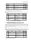
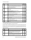
Bit
No.
Mnemonic Description Reset
Value
R/W
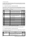
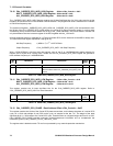
15:8
Not used
.-W
7:0 CHx_CODE_DCO_PRESET_
PHASE [24:16]
More significant bits (25 to 18) of the Code DCO
phase which is to be loaded at the next TIC event in
PRESET mode.
0x00 W
Table 7.19 CORR CHx_CODE_DCO_PRESET_PHASE Register