


6: BSIO Interface
GP4020 GPS Baseband Processor Design Manual 39
Standard and Page Modes, with the width of the Control Word being configurable between 2-bits and 32-bits via
the CWORD bits.
In Standard Mode, the start of an Operation is defined as when the first word is written to the Read/Write Buffer. In
Page Mode, the start of an operation is defined as when the control word is written to the control word buffer.
In case of an Overflow condition (byte / word received when both words of the receive FIFO are full) an error bit
READERR in the Status Register is set. The new byte/word will not be shifted into the receive FIFO. An Under-flow
condition (byte / word required to be transmitted when both words of the transmit FIFO are empty) will result in the
WRITERR bit in the Status Register being set and the previous byte/word being sent.
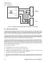
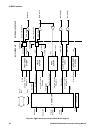
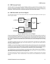
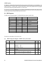
6.3 BSIO Frequency Divider
The Frequency Divider allows the BµILD Bus clock B_CLK, to be divided down to a frequency of between B_CLK/2
to B_CLK/512, depending on the value selected by the SCLKFREQ bits in the Configuration Register. It consists of
a 9-bit Synchronous Counter and SCLK Enable Logic as shown in Figure 6.6 below.
Two outputs are provided: SCLK_INT (the serial output clock) and SCLKX2 (twice the frequency of SCLK_INT).
The frequency divider is disabled and held reset when no operation is currently in progress.
9 BIT
COUNTER
SCLK
ENABLE
LOGIC
SCLKFREQ
B_CLK
SCLKX2
SCLK_INT
SCLK_CTR
SCLK_EN
CPOL
SSEL
SCLKON
OPERATION
Figure 6.6 BSIO Frequency Divider
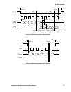
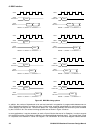
The division ratio of the counter is selected by the SCLKFREQ bits in the Configuration Register, and is in the
range 2^1 to 2^9, for SCLKFREQ = 0000 to SCLKFREQ = 1000 respectively. It is clocked by the Rising Edge of
B_CLK.
SCLK_EN, an output from the Sequencer, is used to enable or inhibit SCLK_INT. When SCLK_INT is in the idle
state (i.e. inhibited), its polarity will be configured for each of the slaves (SS0 & SS1) by means of the CPOL bits in
the Slave Select Register (High if CPOL = 1). The Timing Diagram for this is shown in Figure 6.7 below. Note that
if there is a change in the polarity of SCLK_INT, when selecting between two devices, the start of the first operation
can be delayed as required.