


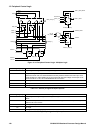
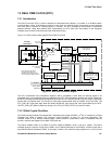

12: Peripheral Control Logic
GP4020 GPS Baseband Processor Design Manual 127
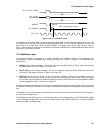
Note: For each change of value of PLL_IN_SEL[1:0] or at PLL wake-up, the PLL will be disabled for a wait
period of approx. 183µs (6 * 32kHz clock cycles, determined by the Real Time Clock block). This allows
the CLKINB to stabilise.
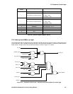
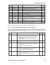
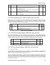
12.7.2 PCL Input / Output Control register - IO_REV - Memory Offset 0x00C
This register combines the control of the Input / Output signal multiplexing on the GPIO[7:0], MULTI_FNIO and
DISCIO pins (Pins 91, 92, 93, 95, 96, 97, 99, 100, 54, 55 respectively in 100-pin package), and a read of the Chip
Revision register. Bits 9:0 can be read as well as written to; by reading the bits, the settings made by the previous
Write can be observed.
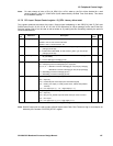
Bit
No.
Mnemonic Description
Reset
Value
R/W
15:10 CHIP_REV[5:0] Read Only Chip Revision number (MSB = Bit 5).
'000000' = Rev 0. First version of GP4020
‘000001’ = Rev 1. Second version , etc.
000000 R
9 EXT_NCS0 '1' = Disable Internal Boot ROM, at reset, if MULTI_FNIO (pin 54 (100-pin
package)) is set High.
'0' = Enable Internal Boot ROM, at reset, if MULTI_FNIO (pin 54 (100-pin
package)) is set High.
0R/W
8 DISCOP_MUX '1' = Connect DISCOP output from 12-channel Correlator to GPIO[5] (pin
93).(
See Note)
'0' = Connect GPIO[5] to GPIO[5] (pin 93).
0R/W
7:6 BSIO_MUX[1:0] Multiplex BSIO connections onto GPIO[3:0] pins.
'00' = GPIO[3:0] connect to GPIO[3:0] input / output pins
'01','10','11' = BSIOCLK connects to GPIO[0] (pin 100 (100-pin package))
BSIODATA connects to GPIO[1] (pin 99 (100-pin package))
'x1' = BSIOSS[0] connects to GPIO[2] (pin 97)
'1x' = BSIOSS[1] connects to GPIO[3] (pin 96)
00 R/W
5:3 MFNIO_CFG[2:0] Multiplex signals onto MULTI_FNIO (pin 54).
'0xx' = Input only
'100' = 100kHz Square wave output (NOT Timemark aligned)
'101' = UART_CLK output (i.e. Firefly system Clock, without sleep disable
function)
'110' = Low output (i.e. '0'); '111' = High output (i.e. '1')
000 R/W
2:0 DISCIO_CFG[2:0] Multiplex signals onto DISCIO (pin 55).
'0xx' = Input only
'100' = RF_PD / RF_SLEEP output to Power-down pin on RF Front-end.
'101' = TIC output
'110' = Low output (i.e. '0'); '111' = High output (i.e. '1')
000 R/W
Table 12.6 PCL IO_REV Register
Note: DISCOP output can be used to output 100kHz Square wave Clock, Raw Timemark, High or Low outputs, as
defined by the Correlator "SYSTEM_SETUP" register.