


12: Peripheral Control Logic
120 GP4020 GPS Baseband Processor Design Manual
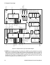
MULTI_FNIO
DISCIO
CLK100KHz
DISCOP_MUX
BSIO_MUX[1:0]
MFNIO_CFG[2:0]
MULTI_FNIO_READ
UART_CLK
'0'
'1'
RF_PD
DISCIO_CFG[2:0]
DISCIO_READ
TIC
'0'
'1'
GPIO[0:7]
BSIO
DISCOP
DISCIP1
GPIO[0:7]
RF_SLEEP
PLLDT1
UIM_TEST
0
1
2
3
4
5
6
7
0
1
2
3
4
5
6
7
SS[1]
SS[0]
DATA
CLK
UIM_TEST
SIGN1
MAG1
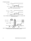
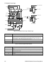
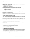
Figure 12.10 Peripheral Control Logic - Multiplex Logic
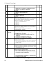
DISCIO_CFG[2:0] DISCIO Function
0xx Input only; read using DISCIO bit in IP_READ register. Also used by Correlator in UIM Test Mode.
100 RF_PD or RF_SLEEP output to RF Front-end.
Note if this mode used, it is recommended that 1kohm pull-down resistor used on this pin, since
reset-condition is to make DISCIO pin an input, which will mean that voltage on PDn input on RF
Front-end will be >+0.8V, and could disable the RF Front-end IC.
101 TIC output
110 '0' output
111 '1' output
Table 12.1 DISCIO pin signal multiplex options
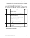
MFNIO_CFG[2:0] MULTI_FNIO Function
0xx Input only; read using MULT_FNIO bit in IP_READ register. Also used by Correlator in UIM Test
Mode.
100 CLK100KHz output from 12-channel correlator block. This signal is a 100kHz square wave, phase-
locked to RF Front-end PLL.
101 UART_CLK output.
110 '0' output
111 '1' output
Table 12.2 MULTI_FNIO pin signal multiplex options