


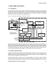
12: Peripheral Control Logic
124 GP4020 GPS Baseband Processor Design Manual
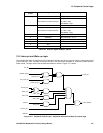
12.6.2 RF Input and RF Front-end Power-Down
A Power-down of an RF Front-end IC, along with disabling the 40MHz Low Level Differential Input cell in the
System Clock Generator, can be made to occur if:
a) RF_PD bit (POW_CNTL[0]) set to '1'.
b) RF_SLEEP bit (POW_CNTL[10]) set to '1'.
Under these conditions, the following pins on the GP4020 (100-pin package) get set as follows:
• Set as High Impedance (i.e. Tristate):
NSCS[0] (pin 11), NSCS[1] (pin 12), NSCS[2A] (pin 13), NSOE (pin 25), NSWE[1] (pin 26), NSWE[0] (pin
27), NSUB (pin 52), SDATA[15:0]
• Set to Logic Low:
SAMPCLK (pin 63), U2TXD (pin 76), U1TXD (pin 78)
In this mode, DISCIO (pin 55) can be configured to output a '1' to power down an RF Front-end IC (achieved if
DISCIO_CFG[2:0] in IO_REV register is set to '100'.
As the 40MHz input from the RF Front End IC is disabled, this option should only be used if the Firefly clock source
is not derived from this. Otherwise, the system will lock up, due to there being no clock-source for the Firefly MF1.
12.6.3 Real Time Clock Crystal Oscillator Cell Disable
The RTC 32kHz crystal-oscillator cell can be disabled by setting IDDQ_TEST (pin 70 (100-pin package)) to High.
The Real Time Clock is NOT disabled by a Full Power Down.
(Note: Setting IDDQ_TEST to High is NOT a mode required in normal operation, and is primarily involved with
manufacturing test of the GP4020. It is used to disable the Crystal Oscillator in the Real Time Clock, and the
Processor Clock Crystal Oscillator, the PLL and the 40MHz Low Level Differential Input cell in the System Clock
Generator).
12.6.4 System Clock Generator Processor Crystal Oscillator cell Disable
The Processor Crystal Oscillator cell in the System Clock Generator, can be disabled by setting PRX_EN bit
(POW_CNTL[1]) to '0';
12.6.5 System Clock Generator Phase Locked Loop (PLL) Disable
The Phase-locked Loop cell in the System Clock Generator, can be disabled by:
1) Setting PLL_PD bit (POW_CNTL[2]) set to '1'.
2) Setting PLL_SLEEP bit (POW_CNTL[9]) set to '1'.
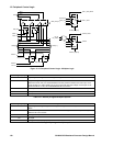
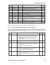
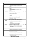
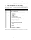
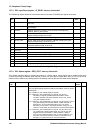
12.7 Peripheral Control Logic Registers
The Peripheral Control Logic uses four registers. Other blocks of circuitry in the GP4020 besides the PCL block use
registers in the address space for the PCL. Reference to all registers in the PCL address space is shown in Table
12.4 below. Those Blocks actually used by the PCL are indicated with the Functional Block designation "PCL". All
registers in Table 12.4 below can be accessed as either byte, half-word, or word.
The GP4020 Peripheral Control Logic Base Address is 0x4010 1000.