


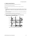

20: Input / Output pin Characteristics
GP4020 GPS Baseband Processor Design Manual 189
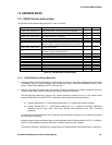
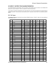
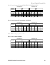
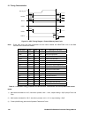
20.3.1.2 Normal N outputs (3.3V outputs): CLAIO1HD01N, CLAIO1NR01N, CLAOP01N.
Input edge 0.1ns Input edge 1.5ns
Switching
Delay (ns)
Load
(pF)
Load
(pF)
10 20 40 80 150 10 20 40 80 150
D → OP ↑
5.82 6.99 8.89 11.75 15.76 5.55 6.72 8.62 11.48 15.49
D → OP ↓
5.55 6.75 8.60 11.18 14.48 6.37 7.56 9.42 11.99 15.30
T → OP ↑
6.10 7.27 9.18 12.05 16.06 6.91 8.08 9.99 12.86 16.87
T → OP ↓
5.49 6.66 8.49 11.04 14.33 6.30 7.47 9.30 11.85 15.15
Table 20.5 X01 Normal N 3.3V Output delays
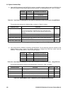
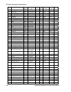
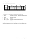
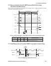
20.3.1.3 Normal N outputs (5V Tolerant outputs): SCJIO1NR01N.
Input edge 0.1ns Input edge 1.5ns
Switching
Delay (ns)
Load
(pF)
Load
(pF)
10 20 40 80 150 10 20 40 80 150
D → OP ↑
6.22 6.99 8.22 10.00 12.38 5.88 6.65 7.88 9.66 12.04
D → OP ↓
8.49 9.42 10.82 12.66 14.86 9.35 10.28 11.68 13.52 15.72
T → OP ↑
6.40 7.17 8.40 10.17 12.56 7.26 8.03 9.26 11.04 13.42
T → OP ↓
7.28 8.19 9.57 11.38 13.57 8.14 9.04 10.42 12.24 14.43
Table 20.6 X01 Normal N 5V Tolerant Output delays
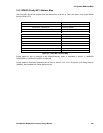
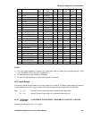
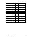
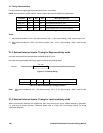
20.3.2 X03 Drive Outputs (x3 Current drive)
20.3.2.1 Slow L1 outputs: CLAOP03L1.
Input edge 0.1ns Input edge 1.5ns
Switching
Delay (ns)
Load
(pF)
Load
(pF)
10 20 40 80 150 10 20 40 80 150
D → OP ↑
6.03 7.72 10.36 14.03 18.74 5.75 7.45 10.09 13.76 18.47
D → OP ↓
8.09 9.52 11.73 14.75 18.56 8.90 10.33 12.54 15.57 19.38
T → OP ↑
6.32 8.02 10.67 14.38 19.16 7.13 8.83 11.49 15.19 19.97
T → OP ↓
8.09 9.51 11.71 14.72 18.52 8.89 10.32 12.52 15.53 19.33
Table 20.7 X03 Slow L1 3.3V Output delays