


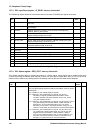
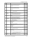

14: System Clock Generator
136 GP4020 GPS Baseband Processor Design Manual
14.2 40MHz Low Level Differential Input
The 40MHz low-level differential input can process the 40MHz signal from a RF Front-end chip. The signal should
have a DC bias of less than approx. 1.7V with respect to GND, and the 40MHz signal should have amplitude of
approx. 100mV at a frequency of 40MHz. As a minimum, the CLK_I and CLK_T signals from the RF Front-end
should be present in order to provide a phase-locked 40MHz M_CLK clock signal to the 12-channel correlator
block. This same M_CLK signal can also be used to generate the UART_CLK (and BµILD_CLK) signal for all the
other GP4020 system blocks, in conjunction with a series of clock selection logic and a Phase-locked-Loop (PLL).
If using the GP4020 in conjunction with a GP201x RF Front-end, care should be observed to ensure that the DC
bias applied to the CLK_T (pin 58 (100-pin package)) and CLK_I (pin 59) inputs of the GP4020 is set correctly. The
maximum output bias of the GP201x RF Front end on the OPCLK+ and OPCLK- signals is Vcc - 0.8V, which could
give a maximum bias of +2.8V (Vccmax = +3.6V).
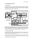
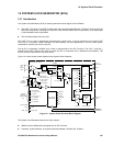
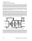
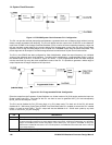
It is recommended that the circuit shown in Figure 14.2 below is used to interface the OPCLK+ / - lines of the
GP2015 RF Front-end to the CLK_T and CLK_I inputs on the GP4020. The PSU configuration for the GP4020
allows the GP4020 to remain powered (using "GP4020 +3.3V") while the remaining circuitry within the GPS
Receiver is powered off (using "Main +3.3V"). The use of 100kΩ resistors is to ensure that the standby current
through the resistors is moderately low (~20µA) while the receiver is powered up, but when "Main +3.3V" is
removed, the current through these resistors will disappear. Also, the A1Vdd pin (Pin 57 (100-pin package)) and the
Vdd supply to the 100kΩ resistors needs to be well de-coupled via wide-band de-coupling to the GND pin at pin 60.
This is to ensure that supply noise is minimised, and that the 40MHz low-level differential input block does not
oscillate. Note that the 100kΩ resistors should be AC-locked to the A1Vdd pin, by means of a 10nF coupling
capacitor between "GP4020 +3.3V" and "Main +3.3V", in close proximity to the A1Vdd pin itself.
100k 100k
100k
10nF
100k
10nF
OPCLK+
OPCLK-
CLK_I
CLK_T
(58)
(59)
GP2015
GP4020
A1Vdd
GND
Vcc
GND
33nF470pF
Vdd
(68)(57)
(60)
10k
Main +3.3V
10nF
GP4020 +3.3V
Figure 14.2 Circuit to interface OPCLK+/- from GP2015 to CLK_T / _I on GP4020
The 40MHz low-level differential block, which generates M_CLK to the correlator core (and optionally the Firefly
MF1 core), is disabled during RF sleep mode, or by RF_PD being high. The power down signal to the differential
cell can also be output on DISCIO pin (if DISCIO configured to output RF_PDOWN, it will be high during power
down). If the differential cell is powered down due to RF_SLEEP, it will be enabled again by a wake-up event. If the
differential cell is powered down by RF_PD bit in the POW_CNTL register, the processor has to manually enable it.
Therefore, if BµILD_CLK to the Firefly MF1 core is derived from M_CLK, the RF_SLEEP mode should not be used.