


11: Memory Peripheral Controller
GP4020 GPS Baseband Processor Design Manual 109
11 MEMORY PERIPHERAL CONTROLLER (MPC)
11.1 Introduction
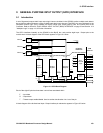
The Memory Peripheral Controller (MPC) is the interface between the BµILD bus and the external bus system. The
MPC is a BµILD bus slave, which performs byte packing and sub memory width writes that allows bus masters to
access external components of different widths, and use variable length read- and write wait-states. This allows the
ARM to connect to nearly any memory component or parallel peripherals needed. The memory interface consists of
a 20-bit address and 16-bit data bus along with the associated control signals.
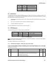
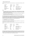
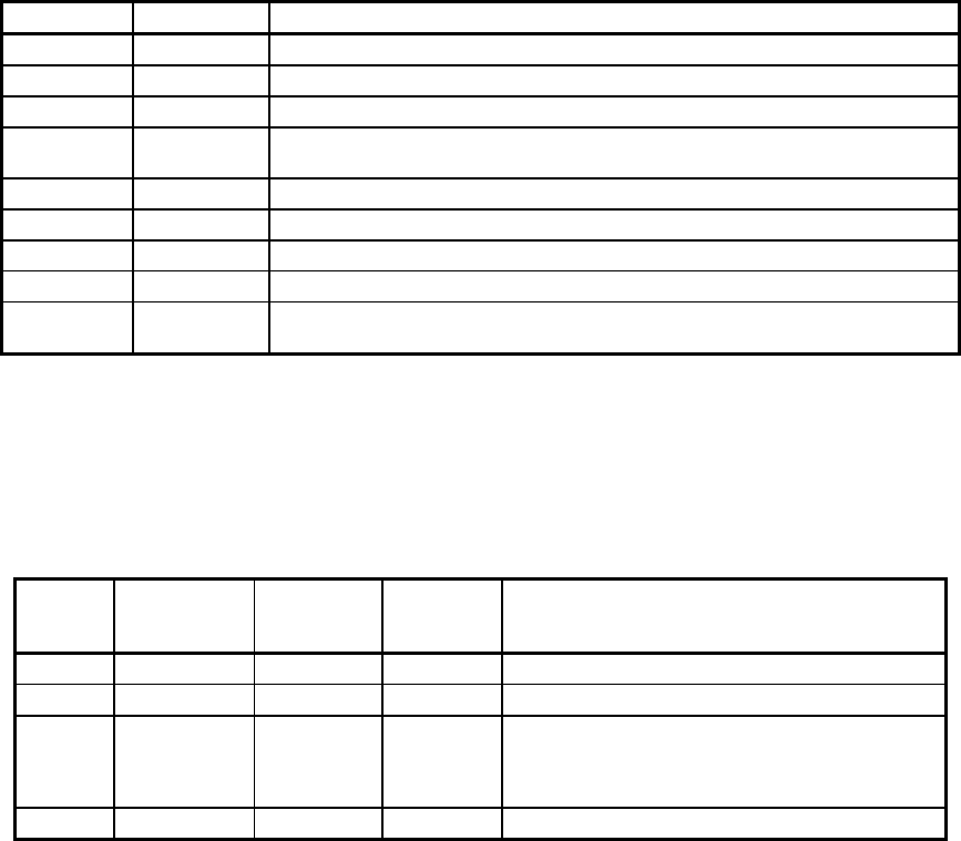
Pin Name Direction Function
NSCS[0} Output Internal & External Boot ROM. Active low.
NSCS[1] Output External Chip Select 1. Active low.
NSCS[2A] Output External Chip Select 2. Active low.
NSWE[1:0] Output
Write Enable, active low. Two provided for use with two 8-bit devices. One used with
a single 8- or 16-bit device.
NSOE Output Output Enable, active low.
SADD[18:0] Output Address Bus
SDATA[15:0] Input / Output Data Bus
SWAIT Input Input, active High. Wait signal. Inserts wait states into current cycle.
NSUB Output Output, active Low. Selects Upper byte for Byte Writes to 16-bit SRAM. SADD[0]
selects Lower Byte, and may be used as such for 8-bit SRAM.
Table 11.1 External Memory Bus Pinout
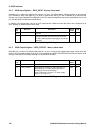
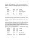
The control of the MPC involves the use of four areas of Configuration, which are covered by four internal select
lines: NCS[0], NCS[1], NCS[2] and NCS[3]. Each of these is configured to drive a separate area of memory in a
GP4020 based system.
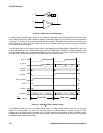
The mapping of the NCS lines to the NSCS lines is not direct, as the data in Table 11.2 below shows.
Address
Offset
Register Firefly MF1
Core select
External
Chip
Select
Function
0x000 Area 1 Config. NCS[0] NSCS[0] Controls Internal / External Boot ROM Memory
0x004 Area 2 Config. NCS[1] NSCS[1] Controls External SRAM memory chip 1
0x008 Area 3 Config. NCS[2] NSCS[2A]
Controls External SRAM memory chip 2A and some
internal components: 12-channel Correlator, 1PPS
Timemark Generator, System Clock Generator, Real
Time Clock and Peripheral Control Logic.
0x00C Area 4 Config. NCS[3] N/A Controls Internal SRAM, ( 2k x 32-bit )
Table 11.2 Memory Peripheral Controller Configuration Registers
The MPC Configuration registers are used to configure the bus-width, the wait-state timing, and the read-only state
of each memory area controlled by the MPC.
11.2 GP4020 Memory Area 1 Configuration
GP4020 Memory Area 1 is at the base of the Address Map (0x0000 0000 through to 0x000F FFFF), and is typically
shared between an internal BOOT ROM and an external 16-bit FLASH EPROM via chip-select line NSCS[0]. The
control of whether the BOOT ROM or the External memory space is selected, is controlled by the state of
MULTI_FNIO (pin 54 (100-pin package)) at chip reset. Refer to Section 4 "BOOT ROM" on page 27 for more
information.