


21: Timing Characteristics
GP4020 GPS Baseband Processor Design Manual 197
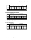
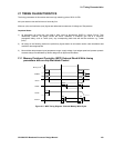
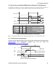
21.6 System Services Module (SSM) Broadcast Diagnostic Timing Diagrams
The SBDIAG lines referred to here are the Xdiag[3:0] lines which can be configured within the SSM to be
multiplexed with the JTAG interface, to allow access to any SADD or SDATA line within the Firefly MF1.
SDATA
BuILD_CLK
Tbgdo
SBDIAG
Tbdiag Tbdiagh
Tbgdoh
Figure 21.6 External Broadcast diagnostic signal (SBDIAG) timings from SSM.
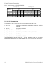
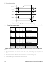
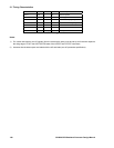
Parameter Typ. units Description and notes
Tbgdo 10.0 ns
Sdata valid after B
µILD_CLK with broadcast
diagnostics enabled
Tbgdoh 8.0 ns
Sdata hold time after B
µILD_CLK with broadcast
diagnostics enabled
Tbdiag 15.0 ns
Bdiag data valid after B
µILD_CLK
Tbdiagh 13.0 ns
Bdiag output data hold time after B
µILD_CLK
Table 21.5 Simulated Broadcast Diagnostic Timing parameters
Note: Typical results simulated for +25°C, typical silicon process, Vdd = +3.3 V, output loading = 50pF.
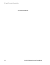
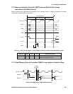
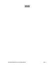
21.7 JTAG interface Timing Diagram
The data for the JTAG interface timing has been copied from Rev 3 of the ARM7TDMI Technical Reference Manual
(document reference ARM DDI 0029F), which is downloadable (1.7 MB PDF) from ARM's website
http://www.arm.com. The documentation download page can be found at:
http://www.arm.com/arm/documentation?OpenDocument .
TMS
TDI
TCK
Tbsih
TDO
Tbsod
Tbscl Tbsch
Tbsis
Tbsoh
Figure 21.7 JTAG Interface Characteristics