


7: 12-Channel Correlator
GP4020 GPS Baseband Processor Design Manual 83
7.6.27 PROG_TIC_HIGH Register - Write Address Offset 0x1B4
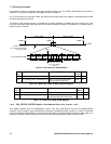
The PROG_TIC_HIGH and PROG_TIC_LOW register locations operate in conjunction to set the period of TIC. TIC
is generated by a 21-bit binary down counter when it reaches zero. It then loads to a Preset value stored in its
Preset register and starts to count down again. If the Preset value is P, the count sequence is P, P–1, P–2, ...,1, 0,
P, P–1. Hence, the counter divides by P+1 producing an output with a period of (P+1) * clock period. Since the TIC
counter is clocked by the multi–phase clock, the clock period is (7 * clock period) (nominally 40MHz i.e. 25ns).
Writing to the PROG_TIC_HIGH/_LOW locations can modify the value stored in the Preset register. This will
overwrite the previous contents of the Preset value. The Preset value is set to be 0x08B823, which gives a nominal
TIC period of 0.0999999seconds exactly (i.e. 100ns short of 100.0000ms, derived by {(571427+1) * 7 / 40MHz}).
The TIC counter may be loaded by writing directly to the PROG_TIC locations. This may be achieved in one of two
ways:
i) PROG_TIC_HIGH value can be written, followed by the PROG_TIC_LOW value, (at which point the full
21-bits are transferred to the Preset register);
ii) PROG_TIC_LOW value may be written to modify the lower 16-bits of the Preset value.
It should be noted that in the former case, the top 5-bits programmed as PROG_TIC_HIGH are stored locally to the
TIC counter. Even if a write to PROG_TIC_LOW does not directly follow the write to PROG_TIC_HIGH, the next
PROG_TIC_LOW write will still transfer all 21-bits. It is also necessary to ensure that the write to PROG_TIC_HIGH
precedes the write to PROG_TIC_LOW, rather than follows it.
The transfer of data to the TIC counter data latches occurs under control of the multi–phase clock write cycle and
the write to the Preset register happens subsequent to the main internal write.
Using the PROG_TIC write locations the TIC period is as follows:
TIC Period = ((PROG_TIC_HIGH * 65536) + PROG_TIC_LOW + 1) * 7 / (40MHZ)
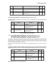
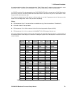
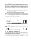
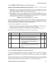
Bit
No.
Mnemonic Description Reset
Value
R/W
15:5
Not used
-W
4:0 PROG_TIC[20:16] Bits 20:16 of the 21-bit TIC Period Register.
Must be written before PROG_TIC_LOW values.
0x08 W
Table 7.33 CORR PROG_TIC_HIGH Register
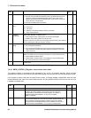
7.6.28 PROG_TIC_LOW Register - Write Address Offset 0x1BC
This register contains the 16 least significant bits for the PROG_TIC register. Refer to "PROG_TIC_HIGH" for more
information.
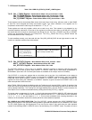
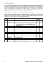
Bit
No.
Mnemonic Description Reset
Value
R/W
15:0 PROG_TIC[15:0] Bits 15:0 of the 21-bit TIC Period Register 0xB823 W
Table 7.34 CORR PROG_TIC_LOW Register
7.6.29 RESET_CONTROL Register - Write Address Offset 0x1FC
This register is used to disable correlator channels which are not required in the navigation solution, and at the
same time undertake a full hardware reset of the channel. By removing multiphase clocks from a disabled channel,
the power-consumption of the 12-channel correlator block can be reduced.
When a CHx_RSTB bit is set Low to disable a correlator channel, the reset bit inhibits propagation of the clock
phases to the CHx tracking channel. It also resets the Accumulated Data flags, Code DCO and Carrier DCO
accumulators, the I & Q accumulators, and the Code Phase Counter. A CHx_RSTB does not reset the Carrier