


GP4020 GPS Baseband Processor Design Manual Index - III
Table of Figures
Page
Figure 1.1 GP4020 Block Diagram ......................................................................................................................2
Figure 1.2 Block Diagram of typical GP4020 based GPS receiver.........................................................................8
Figure 2.1 GP4020 100-pin package pin distribution...........................................................................................11
Figure 2.2 GP4020 100-pin package outline drawing..........................................................................................12
Figure 3.1 ARM7TDMI Architecture ...................................................................................................................20
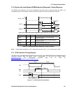
Figure 4.1 Boot ROM UART Download Data Protocol ........................................................................................29
Figure 6.1 Using BµILD Serial Input Output (BSIO) with EEPROM and LCD peripherals .....................................34
Figure 6.2 BµILD Serial Input Output (BSIO) Block Diagram...............................................................................36
Figure 6.3 BSIO Read Operation Timing Diagram..............................................................................................37
Figure 6.4 BSIO Write Operation Timing Diagram..............................................................................................37
Figure 6.5 BSIO Bit timing options.....................................................................................................................38
Figure 6.6 BSIO Frequency Divider ...................................................................................................................39
Figure 6.7 BSIO SCLK Polarity Timing...............................................................................................................40
Figure 6.8 BSIO Slave Select Logic...................................................................................................................40
Figure 6.9 BSIO Write Buffer and Control Register.............................................................................................41
Figure 6.10 BSIO Read Buffer...........................................................................................................................42
Figure 6.11 BSIO Sequencer.............................................................................................................................43
Figure 7.1 12-Channel Correlator Block Diagram ...............................................................................................50
Figure 7.2 Tracking Module Block Diagram........................................................................................................52
Figure 7.3 Waveform outputs from Carrier DCO I & Q LO (sinewaves are a guide only) ......................................53
Figure 7.4 Integrated carrier phase....................................................................................................................63
Figure 7.5 Slew timing in UPDATE Mode...........................................................................................................76
Figure 9.1 GPIO Block Diagram ......................................................................................................................103
Figure 9.2 GPIO Pad Cell Configuration...........................................................................................................104
Figure 9.3 GPIO BµILD Bus interface timing ....................................................................................................104
Figure 12.1 Peripheral Control Logic Top-level Block Diagram .........................................................................114
Figure 12.2 Peripheral Control Logic - Reset Logic...........................................................................................115
Figure 12.3 RF_PLL_LOCK Hardware Reset Generation .................................................................................116
Figure 12.4 POWER_GOOD Hardware Reset Generation when POWG_EN = '0', and UART_CLK NOT derived
from an RF Front-end.......................................................................................................................................116
Figure 12.5 POWER_GOOD Hardware Reset Generation when POWG_EN = '1'. Assumes that power to RF
Front-end fails, and RF_PLL_LOCK is low for upto 5ms after power-up.............................................................116
Figure 12.6 NSRESET Hardware Reset Generation.........................................................................................117
Figure 12.7 Watchdog Hardware Reset Generation .........................................................................................117
Figure 12.8 SFT_RESET Hardware Reset Generation .....................................................................................117
Figure 12.9 PLL_ENABLE Timing....................................................................................................................119