


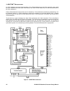
4: Boot ROM
28 GP4020 GPS Baseband Processor Design Manual
0000, and the ROM space from 0x6000 0000. The ARM7TDMI will then begin execution of code downloaded
to the Internal RAM, starting at address 0x6000 0000.
The EXT_NCS0 bit in the IO_REV register (within the PCL) can then be set so that Firefly NCS[0] signal selects
external NSCS[0] instead of internal boot-ROM. Remember that NSCS[0] will now start at address 0x6000 0000
due to MPC swap.
The Memory space swap implemented by the boot ROM can be cleared by a GP4020 reset, due to:
1) RF_PLL_LOCK (pin 56 (100-pin package)) going Low, with EN_PLL_RST set to '1' (bit 7 of PER_STAT
register in PCL);
2) POWER_GOOD (pin 64 (100-pin package)) going Low, with EN_POW_RST set to '1' (bit 6 of PER_STAT
register in PCL);
3) SFT_RESET set to a '1' (bit 4 of PER_STAT register in PCL);
This will cause the MPC swap function to revert to NCS[0] appearing at address 0x0000 0000, and NCS[3]
appearing at address 0x6000 0000. However, these three reset sources will not effect whether NCS[0] selects
internal boot-ROM or external NSCS[0] device.
4.2 UART Download Data Protocol
The nominal UART1 speed is set to be ~57.6Kbaud, and the UART clock is derived from the 40MHz CLK_T and
CLK_I signals from the RF Front-end IC. The UART clock is 20MHz, and the UART1 Baud-Rate-Register is set to
produce a 16 x Baud Rate of 0.90909MHz. The actual baud rate is 56.8kBaud, which is in error by -1.3%.
The protocol to be used for downloading data to the GP4020 is detailed below. The main purpose of the protocol is
to provide simple but reliable data transfer. The protocol does not include any error checking. Any error checking on
the downloaded code can be performed by the downloaded code itself when it starts to execute. This has two
advantages:
1) It keeps the download protocol simple.
2) It allows maximum flexibility in the error checking routines that can be implemented.
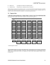
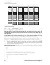
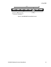
The data protocol has three Header Bytes. These provide an indication of the number of Data Bytes (N) which are
to be transmitted and hence stored in the internal RAM area of the GP4020 (this number excludes the three header
bytes). The first header Byte (Byte 1) is the most significant data for a 24-bit number, Byte 2 is the next most
significant and Byte 3 is the least significant.
Once the header Bytes have been transmitted, the data bytes can be sent. The boot ROM will cycle through a
retrieve-and-store routine for each byte in the transmitted data, upto a total of N times. Each data byte will be stored
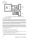
in the Internal RAM. Figure 4.1 below shows the structure of the download data.
When the last byte has been transmitted, the internal ROM and internal RAM address areas are swapped and
program execution will then start from address 0x0000 0000 in internal RAM. This is achieved by swapping Firefly
Chip select lines NCS[0] and NCS[3], so effectively the internal Boot ROM will appear at address 0x6000 0000.