


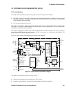
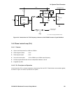

14: System Clock Generator
GP4020 GPS Baseband Processor Design Manual 143
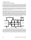
UART
_CLK
O/P
Freq.
(MHz)
I/P
Freq.
MHz
PLL
Mult
Fact
Prog.
Divider
setting
DIV
[4:0]
Charge
Pump
setting
CHP
[4:0]
PLL
SYNC
MODE
SYN
CEN
PLL
O/P
VCO
Freq.
MHz
VCO
Freq.
Range
VCOD
[1:0]
BY-
PASS
PLL
PLL_
BYP
PLL
O/P
Divide
Factor
B_
CLK
_SEL
[1:0]
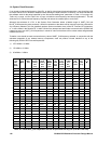
Ts
3
(µs)
31.25 10.0
1
25 10111 10001 0 250 00 0 8 11 30
32.5 10.0
1
13 01011 01001 0 130 00 0 4 10 44
35.0 10.0
1
7 00101 01001 0 70 01 0 2 01 44
37.5 10.0
1
15 01101 01010 0 150 00 0 4 10 41
40.0
4
20.0
2
4 00010 00101 0 80 01 0 2 01 67
42.5 10.0
1
17 01111 01011 0 170 00 0 4 10 38
45.0 10.0
1
9 00111 00110 0 90 00 0 2 01 58
47.5 10.0
1
19 10001 01101 0 190 00 0 4 10 35
50.0
4
10.0
1
10 01000 01101 0 100 01 0 2 01 35
52.5 10.0
1
21 10011 01110 0 210 00 0 4 10 33
55.0 10.0
1
11 01001 00111 0 110 00 0 2 01 52
57.5 10.0
1
23 10101 01111 0 230 00 0 4 10 32
60.0
4
20.0
2
6 00100 00100 0 120 00 0 2 01 81
62.5 10.0
1
25 10111 10001 0 250 00 0 4 10 30
65.0 10.0
1
13 01011 01001 0 130 00 0 2 01 44
70.0
4
10.0
1
14 01100 01001 0 140 00 0 2 01 44
Table 14.3 Higher UART_CLK frequencies that can be produced from M_CLK – not recommended for
normal operation
Notes (for table 14.2 and 14.3):
1) When PLL input frequency is 10.0MHz, this is derived by dividing M_CLK by 4, using PLL_IN_SEL[1:0] set to
'11'
2) When PLL input frequency is 20.0MHz, this is derived by dividing M_CLK by 2, using PLL_IN_SEL[1:0] set to
'10'.
3) Ts = Worst-case settling time.
4) It is important to ensure that UART_CLK maintains a duty cycle as close as possible to 50:50. This can be
achieved by deriving direct multiples of 10MHz over multiplying by a factor of 2, and then dividing the PLL
output by 2 accordingly.
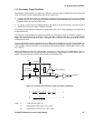
Table 14.4 below shows some register values for PLL_CNTL and POW_CNTL, to produce some typical
UART_CLK frequencies, based on using an RF Front-end M_CLK as a frequency reference. The values already
shown in Table 14.2 on page 142 are used as a basis for the register values shown. Note that the values used in
POW_CNTL register assume that:
1) POWER_GOOD disables ALL functions except Real Time Clock when at logic Low (i.e. Bit 15 is set to ‘1’.
2) Watchdog function is disabled (i.e. bit 14 is set to ‘0’)
3) ALL Wake-up event control bits are de-activated (i.e. bits 13:11 are set to ‘0’)
4) ALL Sleep enable bits are de-activated (i.e. bits 10:8 are set to ‘0’)
5) Processor Crystal Oscillator block is disabled (i.e. bit 1 is set to ‘0’).