


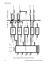

6: BSIO Interface
44 GP4020 GPS Baseband Processor Design Manual
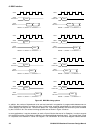
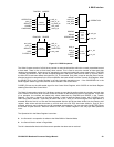
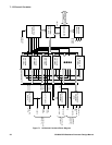
The Sequencer enables SCLK and the Slave Select Logic by means of SCLK_EN and ext_sel respectively. The
bits SSLEAD in the Configuration Register select a delay between the external select being active and SCLK being
enabled of between 1 to 4 SCLK cycles. Similarly the bits SSLAG, select the delay between SCLK being stopped
and the external select being disabled of between 1 to 4 SCLK cycles.
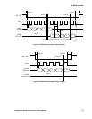
RX_CLK and TX_CLK, the shift register clocks to the Read and Write Buffers are provided to allow data to be sent
or received at either the rising or falling edge of SCLK. RDPOL, WRPOL and SSEL select the clock polarity for read
and write cycles for each of the slave select outputs SS0 and SS1.
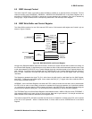
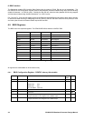
6.9 BSIO Registers
The BSIO uses nine separate registers. The GP4020 BSIO Base Address is 0xE000 7000.
Address Offset Register Direction Function
0x000
CONFIG
Read/Write Configuration Register
0x004
TRSFR
Read/Write Transfer Control Information
0x008
MODE
Read/Write Mode Register
0x00C
-
-
Reserved
0x010
SLAVE0
Read/Write Slave Select 0
0x014
SLAVE1
Read/Write Slave Select 1
0x018 to 0x02C - -
Reserved
0x030
STATUS
Read Status Register
0x034
INTC
Read/Write Interrupt Control
0x038
RWBUF
Read/Write Read Write Buffer
0x03C
CWBUF
Read/Write Control Word Buffer
0x040 to 0xFFC
-
-
Reserved
Table 6.2 BSIO Register Map
All registers are addressable as 32-bit locations only
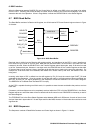
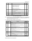
6.9.1
BSIO Configuration Register - CONFIG - Memory Offset 0x0000
Bit Mnemonic Description Reset
Value
R/W
31:18
Reserved
All = 0 R
17:15 SSEL Slave Select. Selects slave as follows:
SSEL=000 SS0
SSEL=001 SS1
ALL OTHERS Reserved
000 R/W
14
Reserved
0R/W
13
Reserved
0R/W
12 CONFSDIO Configure SDIO. A High configures SDIO as an Open Drain
Output, whereas a Low configures it as a CMOS output.
0R/W
11 CONFSCLK
Configure SCLK. A High configures SCLK as an Open Drain
output, whereas a Low configures it as a CMOS output.
0R/W