


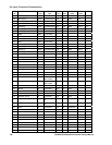

19: System Address Map
182 GP4020 GPS Baseband Processor Design Manual
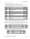
a) Gate NSCS[2A] externally with SADD[19] to produce a smaller external address space for NSCS[2A], but
without the reflection of the internal logic once every 0x2000. The truth-table shown in Table 19.2 below:
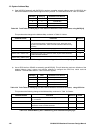
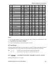
NSCS[2A] SADD[19] EXTERNAL CHIP SELECT
0 1 0 (ENABLED)
0 0 1 (DISABLED)
1 1 1 (DISABLED)
1 0 1 (DISABLED)
Table 19.2 Truth Table for NSCS[2A] to avoid external reflection of internal accesses, using SADD[19]
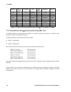
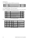
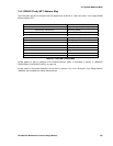
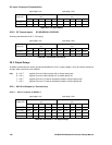
This produces the change to the Address-Map, as shown in Table 19.3 below:
ADDRESS RANGE FUNCTION MPC Area
0x4000 0000 - 0x4007 FFFF Reserved
(12-Channel Correlator, Peripheral Control Logic, Real Time Clock,
System Clock Generator, 1PPS Timemark Generator reflected every
0x2000)
3
0x4008 0000 - 0x400F FFFF External Chip Select 2A via NSCS[2A], gated with SADD[19] = "1" 3
0x4010 0000 - 0x4010 0FFF 12-Channel Correlator 3
0x4010 1000 - 0x4010 1FFF
Peripheral Control Logic, Real Time Clock, System Clock Generator,
1PPS Timemark Generator
3
0x4010 2000 - 0x5FFF FFFF
Reserved (CS2, Correlator, Peripherals reflected)
Table 19.3 GP4020 Memory Area 3 Addressing, with modified NSCS[2A] logic
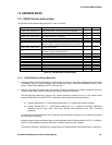
b) Use a GPIO line from GP4020 to externally gate NSCS[2A]. This will allow the maximum utilisation of the
external Memory Area 3 space, but requires software to configure the GPIO line, which could be
inefficient. The truth-table shown in Table 19.4 below applies:
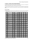
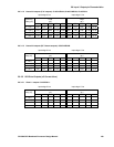
NSCS[2A] GPIO EXTERNAL CHIP SELECT
0 1 0 (ENABLED)
0 0 1 (DISABLED)
1 1 1 (DISABLED)
1 0 1 (DISABLED)
Table 19.4 Truth Table for NSCS[2A] to avoid external reflection of internal accesses, using GPIO line
This produces the following change to the Address-Map, as shown in Table 19.5 below:
ADDRESS RANGE FUNCTION MPC Area NOTES
0x4000 0000 - 0x400F FFFF
External Chip Select 2A via NSCS[2A], gated with GPIO =
"1", in software.
32
0x4010 0000 - 0x4010 0FFF 12-Channel Correlator 3 2
0x4010 1000 - 0x4010 1FFF Peripheral Control Logic, Real Time Clock, System Clock
Generator, 1PPS Timemark Generator
32
0x4010 2000 - 0x5FFF FFFF
Reserved (CS2, Correlator, Peripherals reflected)
Table 19.5 GP4020 Memory Area 3 Addressing, with modified NSCS[2A] logic