


9: GPIO Interface
GP4020 GPS Baseband Processor Design Manual 105
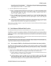
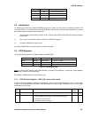
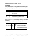
B_SIZE[1:0] Data size B_ERROR
00 8-bit Error, bus error asserted
01 16-bit Error, bus error asserted
10 32-bit Valid, bus error negated
11 Reserved Error, bus error asserted
Table 9.1 GPIO B_ERROR signal
9.2 Initialisation
On power-up, the three bus signals B_MODE[2:0] assume a status of (0,0,0). Also of interest are states of INI
(0,1,0) and RST (0,1,1) which denote a bus-wide initialisation request and a soft reset state respectively. In case of
any of these three bus conditions, the module will:
i) asynchronously initialise with a direction of 'IN' on all bits of the DIRECTION REGISTER (which will tristate
the I/O pins);
ii) set a value of '0' on all bits of both the INPUT and OUTPUT Registers.
iii) Tri-state the BµILD Bus signal drivers.
All other B_MODE states are ignored (normal run state assumed).
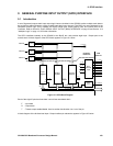
9.3 GPIO Registers
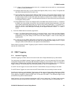
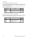
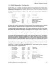
The GP4020 GPIO interface has a Base Address of 0xE000 5000.
Address Offset Register Direction Function
0x000 Direction Read / Write 1 = input, 0 = Output
0x004 Input Read Data from pins
0x008 Output Write Data to pins if Direction = Output
Table 9.2 GPIO Register Map
note: Any read or write access to the unused address, or writes to Input Register, or reads from Output Register
will cause B_ERROR to be asserted high.
All registers are addressable as 32-bit locations only.
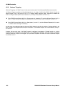
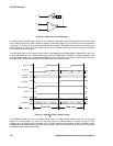
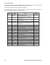
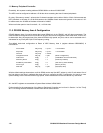
9.3.1 GPIO Direction Register – GPIO_DIR - Memory Offset 0x000
A write to this port enables or disables the corresponding data bit driver to the external pin. Logic '1' disconnects
the pin as in a high-impedance ('Z') state, which then acts as an input. A logic '0' enables drive to the pin, which
then behaves as an output.
Bit
No.
Mnemonic Description
Reset
Value
R/W
31:8 -
Reserved - -
7:0
GPIO_DIR[7:0]
GPIO Pin Direction. Each GPIO_DIR bit maps to a single GPIO signal.
(i.e. GPIO_DIR[4] maps to GPIO[4] - (pin 95 (100-pin package)))
'1' configures the pin as an input,
'0' configures the pin as an output.
0xFF R/W
Table 9.3 GPIO_DIR Register