


21: Timing Characteristics
GP4020 GPS Baseband Processor Design Manual 193
21 TIMING CHARACTERISTICS
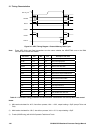
The timing parameters in this section assume a logic switching point of 50% of VDD:
All inputs assume rise and fall times of nominally 2ns.
Minimum (min) and maximum (max) figures are referenced at extremes of Voltage and Temperature.
Important Notes:
1) All parameters will scale from their MIN to MAX value as temperature RISES or voltage FALLS. Their
relationship, however, will always remain the same. Therefore, if conditions give rise to a maximum
propagation delay, such as Taddr (max), any corresponding hold times will also be maximum e.g. Tnweh
(max).
2) All timings in the following section are preliminary figures based on simulation results under worst/best case
conditions where appropriate.
3) Min and Max delays depend upon temperature range, supply voltage, input edges speed and process spreads.
Accurate delays are calculated by Zarlink design kits on approved simulators.
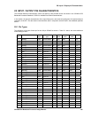
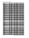
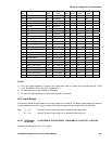
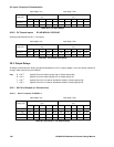
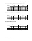
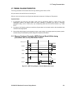
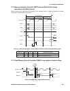
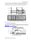
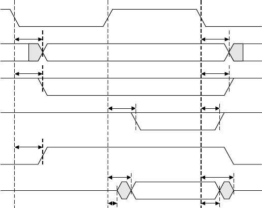
21.1 Memory Peripheral Controller (MPC) External Read & Write timing
parameters with on-chip Wait-state Control
SDATA
NSOE
NSWE
NSCS
SADDR
BuILD_CLK
Taddrh
Tncs
Tnoeh
Tnwe
Tdo
Tde
Taddr
Tncsh
Tnweh
Tdoh
Tdz
Figure 21.1 MPC Timing Diagram - External Memory Write Cycle