


12: Peripheral Control Logic
118 GP4020 GPS Baseband Processor Design Manual
either WATCH_TM or NSRESET signals. Therefore, a complete GP4020 reset can only occur if an NSRESET
or a WATCH_TM event is introduced. These are synchronised to the 32kHz clock developed by the Real Time
Clock, and the resulting output is active low. Additionally, the Reset status bits in PER_STAT[4:0] will only be
reset by an asynchronous NSRESET event or a set of the CLR_RST bit to '0' in PER_STAT register, and will
NOT be cleared by any other reset. An activation of NPOR_RESET will disable any System Clock settings
using the PLL, and consequently, the System Clock will return to 20MHz (M_CLK / 2) when the reset is
released.
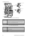
2) NRESET. Used to reset the 12-channel correlator, the Firefly MF1 and all BµILD bus modules. It is derived
from either: NPOR_RESET, RF_PLL_LOCK and POWER_GOOD inputs, or a Software Reset signal
SFT_RESET. This reset line is activated for every type of reset input, and is synchronised to the Firefly Clock
(UART_CLOCK), in conjunction with a 3-cycle delay. An activation of NRESET independent of NPOR_RESET
will NOT disable the System Clock settings using the PLL, but will inhibit the BµILD CLK to the Firefly MF1
Core, and hence power down the Firefly MF1.
There are three areas of the GP4020 where a hard reset resulting in either an NPOR_RESET or NRESET signal,
has no effect:
1) Real Time Clock counters:
a) RTC_PRE[15:1] in the RTC_PRE register
b) All data bits in register RTC_SEC_B
c) RTC_SEC_T[7:0] in the COMPS_RTCS register
The only way the Real Time Clock Counters can be reset is to write a '0' to bit 0 of the RTC_PRE register
(refer to Section 13 "REAL TIME CLOCK (RTC)" on page 131, for more information).
2) Data Retention Register in 1PPS Timemark Generator (TIC_RET[15:8]). There is no asynchronous reset
signal for the Data Retention Register.
3) Internal SRAM (2k x 32-bit).
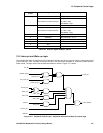
12.3 PLL Enable Logic
An enable line (PLL_ENABLE) is used to re-enable the PLL block in the System Clock Generator after a reset, due
to:
1) PLL Power-down, due to PLL_PD being active and then cleared.
2) PLL Sleep, due to PLL_SLEEP being active and then cleared by a "Wake-up" event.
3) Master Reset due to NRESET being active.
4) Change of PLL frequency due to a change of input reference frequency, controlled by a new setting on
PLL_IN_SEL[1:0].
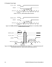
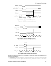
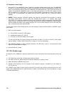
PLL_ENABLE uses a delay of seven cycles of the Real Time Clock (upto 183µs) to ensure that the PLL clock
output is only enabled after the PLL output frequency is stable on the GP4020 chip. The timing diagram in Figure
12.9 below illustrates this.