


7: 12-Channel Correlator
64 GP4020 GPS Baseband Processor Design Manual
7.5.1 Write Cycle To Read Cycle Timings
As described previously, the internal write cycle of the Correlator takes 300ns. Only once the write cycle is
complete will the correlator address decoders switch to decoding the current address. The correlator uses a pre–
charged internal data out bus and hence the decoded address lines must be stable before the internal bus drivers
are enabled (when the read strobe goes high). Consequently, the read strobe must be held Low until some time
after the end of the 300ns (314ns) internal write cycle, to allow sufficient internal address set-up time
7.5.2 Write Cycle To Write Cycle Timings
The internal write cycle of the correlator takes 300ns after the falling edge of the write strobe. During this time the
write internal address and data busses (latched by write) must not be modified. If a second write follows the first,
the second write cycle must be delayed such that it ends no earlier than 300ns after the end of the previous write.
The ‘end’ being a falling edge on the internal write strobe. The specific interface signal timings must also be met.
Writes to the Correlator register X_DCO_INCR_HIGH need not incur subsequent delays, since writes to this
location do not instigate an internal write cycle. A write to this address must always be followed by a write to either
a CHX_CARRIER_DCO_INCR_LOW or a CHX_CODE_DCO_INCR_ LOW register. It is this second associated
write which instigates the internal write cycle.
Note that the exact number of wait states which need to be inserted after a correlator write is not fixed. If the
processor were to perform a correlator write then spend 400ns accessing a different peripheral, subsequent
correlator reads and writes would incur no additional delay.
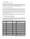
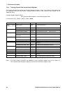
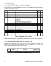
7.6 12-Channel Correlator Register Maps
The register map of the 12-Channel Correlator within the GP4020 is shown in Table 7.2 below. The Base Address
for the GP4020 12-channel Correlator block is 0x4010 0000. The addresses are complete, and it should be noted
that all the register addresses are 32-bit word–aligned but are 16-bits wide, i.e. A0 and A1 are not used. Adjacent
register addresses thus increment by four. Data can be written to and read from the correlator in 32-bit width, but
the 16MSBs of each 32-bit read or write will be ignored.
Address Offset Register Direction Function
0x000 to 0x01C CH0 Control
(see Table 7.3)
Correlator Channel Control Registers
(see Table 7.3)
0x020 to 0x03C CH1 Control
(see Table 7.3) (see Table 7.3)
0x040 to 0x05C CH2 Control
(see Table 7.3) (see Table 7.3)
0x060 to 0x07C CH3 Control
(see Table 7.3) (see Table 7.3)
0x080 to 0x09C CH4 Control
(see Table 7.3) (see Table 7.3)
0x0A0 to 0x0BC CH5 Control
(see Table 7.3) (see Table 7.3)
0x0C0 to 0x0DC CH6 Control
(see Table 7.3) (see Table 7.3)
0x0E0 to 0x0FC CH7 Control
(see Table 7.3) (see Table 7.3)
0x100 to 0x11C CH8 Control
(see Table 7.3) (see Table 7.3)
0x120 to 0x13C CH9 Control
(see Table 7.3) (see Table 7.3)
0x140 to 0x15C CH10 Control
(see Table 7.3) (see Table 7.3)
0x160 to 0x05C CH11 Control
(see Table 7.3) (see Table 7.3)
0x180 to 0x19C MULTI Control
(see Table 7.3) (see Table 7.3)
0x1A4 X_DCO_INCR_HIGH Write
0x1AC PROG_ACCUM_INT Write ACCUM_INT Period Counter
0x1B4 PROG_TIC_HIGH Write Bits [20:16] of TIC Period Counter
0x1BC PROG_TIC_LOW Write Bits [15:0] of TIC Period Counter