


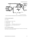

14: System Clock Generator
146 GP4020 GPS Baseband Processor Design Manual
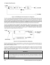
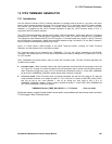
5) Output frequency of PLL; the higher the output frequency, the more current consumed:
i. 240MHz = 6.2mA;
ii. 125MHz = 4.5mA;
iii. 60MHz = 3.4mA;
iv. 30MHz = 2.9mA
As a general rule of thumb, the lower the PLL input frequency, the lower the PLL output frequency and the lower
the UART_CLK divider ratio, the lower the power-consumption of the SCG.
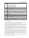
14.6 System Clock Generator Registers
The System Clock Generator uses one primary register, and one register that is shared with functions within the
Peripheral Control Logic block (PCL). The Power Control (POW_CNTL) register is actually documented in Section
12.7.1 "PCL Power Control Register - POW_CNTL - Memory Offset 0x008" on page 125, but the System Clock
Generator functions, associated with this register are documented here. All registers in Table 14.6 below can be
accessed as either byte, half-word, or word.
The GP4020 System Clock Generator Base Address is 0x4010 1000.
Address
Offset
Register Direction Function
0x008 POW_CNTL Read/Write Power Control Register
(shared with Peripheral Control Logic)
0x00A PLL_CNTL Read/Write PLL Control Register
Table 14.6 System Clock Generator Register Map
14.6.1 SCG Power Control Register - POW_CNTL - Memory Offset 0x008
A write to this register stores logic values which set or reset various enable/disable and switching options within the
System Clock Generator. A read of this register shows the status of these functions.
Bit
No.
Mnemonic Description Reset
Value
R/W
15:11 -
Reserved for use in Peripheral Control Logic - -
10 RF_SLEEP
'1' = Disable 40MHz low-level differential input in System Clock Generator,
and apply an active High power-down signal to the RF Front-end (via
DISCIO (pin 55), if so configured (ref. IO_REV register). Can be re-
enabled by a wake-up event (See Note).
'0' = no effect
0R/W
9 PLL_SLEEP '1' = Disable and reset the PLL in System Clock Generator. Can be re-
enabled by a wake-up event (See Note) after a wait period of approx.
183
µs (6 * 32kHz clock cycles; determined by the Real Time Clock
block). This allows the CLKINB to stabilise.
'0' = no effect
0R/W
8-
Reserved for use in Peripheral Control Logic
--