


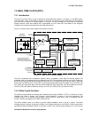

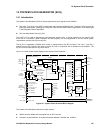

12: Peripheral Control Logic
128 GP4020 GPS Baseband Processor Design Manual
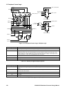
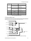
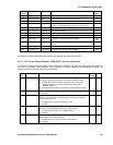
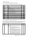
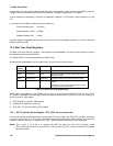
12.7.3 PCL Input Read register - IP_READ - Memory Offset 0x00E
This Read-only register allows the most recent state of a number of GP4020 input signals to be read.
Bit
No.
Mnemonic Description Reset
Value
R/W
15 PER_INT
PER_INT interrupt line, sourced by Peripheral Control Logic to Firefly
MF1 core.
-R
14 DISCIP1 DISCIP1 input to Correlator; can be accessed from GPIO[4] (pin 95 (100-
pin package))
-R
13 DISCOP
DISCOP output from Correlator; can be accessed on GPIO[5] using
DISCOP_MUX (IO_REV register)
-R
12 DISCIO DISCIO input (pin 55 (100-pin package)), if DISCIO_CFG[2:0] in IO_REV
register configured DISCIO as an input.
-R
11 POWER_GOOD POWER_GOOD input (Pin 64 (100-pin package)) - R
10 MULTI_FNIO MULTI_FNIO (pin 54 (100-pin package)), if MFNIO_CFG[2:0] in IO_REV
register configured MULTI_FNIO as an input.
-R
9 TIC TIC output from 12-channel Correlator. Also available from bit 13 in
Correlator register ACCUM_STATUS_B.
-R
8 TIMEMARK 1PPS Timemark output (NOT Raw_Timemark) - R
7:6 Reserved -
5 MAG0 MAG0 data (pin 62 (100-pin package)) from RF Front-end. - R
4 SIGN0 SIGN0 data (pin 61 (100-pin package)) from RF Front-end - R
3 Reserved -
2 TESTMODE Test mode input (pin 74 (100-pin package)) - R
1 Reserved -
0 RF_PLL_LOCK RF_PLL_LOCK input (pin 56 (100-pin package)) from RF Front-end. - R
Table 12.7 PCL IP_READ Register
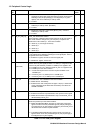
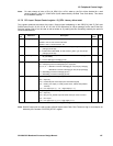
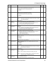
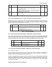
12.7.4 PCL Status register - PER_STAT - Memory Offset 0x010
This register contains flags to indicate the source of a Reset signal, some control bits to disable some reset
sources, some flags to indicate some Interrupt sources and some bits to disable them. Bits [15:11] & [7:5] can be
read as well as written to; by reading the bits, the settings made by the previous Write can be observed.
Bit
No.
Mnemonic Description Reset
Value
R/W
15:14 TIC_INT_EN[1:0] Enable TIC_INT interrupt from 1PPS Timemark Generator. Control of the
TIC_INT signal interrupt within the Overflow Control Block of the TIC Period
slewing logic.
'00' = Disable TIC_INT and RELOAD_TIC signals
'01' = Enable TIC_INT and RELOAD_TIC signals. TIC_INT and
RELOAD_TIC signals generated each time Modulo 7 adder
overflows. Automatic TIC period extension occurs. ADJ_TIC bit
(TIC_RET Register) set also.
'10' = Enable TIC_INT and RELOAD_TIC signals. TIC_INT and ADJ_TIC bit
(TIC_RET Register) set each time Modulo 7 adder overflows. A
Read of ADJ_TIC and subsequent write to ADJ_TIC will set
RELOAD_TIC and cause a TIC period extension. If ADJ_TIC not
written to, no RELOAD_TIC generated and TIC will not be extended.
'11' = Enable TIC_INT and RELOAD_TIC signals. TIC_INT set for every
TIC, irrespective of adder overflow state. ADJ_TIC bit (TIC_RET
Register) set each time Modulo 7 adder overflows. A Read of
ADJ_TIC and subsequent write to ADJ_TIC will set RELOAD_TIC
and cause a TIC period extension. If ADJ_TIC not written to, no
RELOAD_TIC generated and TIC will not be extended.
00 R/W