


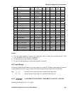
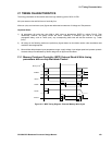


21: Timing Characteristics
194 GP4020 GPS Baseband Processor Design Manual
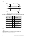
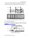
SDATA
NSOE
NSWE
NSCS
SADDR
BuILD_CLK
Taddrh
Tncs
Tnoe
Taddr
Tncsh
Tdih
Tnoeh
Tdisu
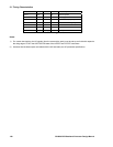
Figure 21.2 MPC Timing Diagram - External Memory Read Cycle
Note: These MPC Write and Read transactions are the same whether the ARM7TDMI core or the DMA
Controller is the current bus master.
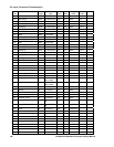
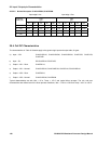
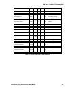
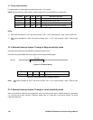
Parameter Min Max Unit Description and notes
Tsclk 14.0 ns
B
µILD Clk low period
Tsclkh 14.0 ns
B
µILD Clk high period
Taddr 12.2 31.5 ns
B
µILD Clk to Address Valid
Taddrh 10.7 28.0 ns Address hold after Sclk
Tncs 11.6 30.0 ns
B
µILD Clk to chip select valid
Tncsh 10.5 27.6 ns Chip select hold after Sclk
Tnoe 13.1 33.0 ns
B
µILD Clk to output enable active
Tnoeh 10.7 27.7 ns Output enable hold after Sclk
Tnwe 9.4 24.4 ns
B
µILD Clk to Write enable
Tnweh 9.9 26.0 ns Write enable hold after Sclk
Tdisu -2.0 - ns Data setup before Sclk
Tdih 7.5 - ns Data input hold time
Tde 9.5 30 ns Data enable time after Sclk
Tdo 12.8 31.6 ns Data valid time after Sclk
Tdz 11.4 29.3 ns Data disable time after Sclk
Tdoh 10.8 28.4 ns Data out hold time after Sclk
Table 21.1 Simulated Timing parameters for MPC External Transactions with on-chip Wait-state control
Notes:
1) MIN results simulated for -40°C, fast silicon process, Vdd = +3.6V, output loading = 50pF (except Tdisu and
Tdih).
2) MAX results simulated for +85°C, slow silicon process, Vdd = +3.0 V, output loading = 50pF.
3) Tnweh (NSWE rising) will ALWAYS precede Taddrh and Tncsh.